Auxiliary Circuitry
The Ultimate Audio Amp
From Genesis to Revelation

Several important functions are implemented under the generic "Auxiliary Circuitry" name. While these features are certainly adding complexity to the whole design, they cannot be avoided if we want a high performance and reliable amplifier. We will analyze these requirements and their current implementations in the following pages.
Inrush current protection
As discussed here, the PGP uses two power toroids of about 300W nominal power each. Compared with standard power transformers, toroidal power transformers have certain advantages regarding the stray magnetic fields (which may drastically impact the overall performance, as further discussed here), the overall size and the magnetic properties. A consequence of the superior magnetic properties of a toroidal transformer is that the transformer "remembers" what polarity the primary voltage had immediately before the power was last shut off. Whenever the voltage has the same polarity when the transformer next is turned on, the core will saturate for part of a half-cycle, and a high inrush current will flow in the primary of the transformer. This inrush current is much larger than the inrush current in a conventional transformer, but it is of a short duration. It can cause an incomfortable light dimming due to an external voltage dip and potentially blow the mains fuses.
One solution is to use a power thermistor in series with the primaries. This was shown as suboptimal if the main power supply is non-regulated. The thermistor will introduce a slight voltage modulation (as a function of the output power). Depending on the performance target, and given the PSRR of the amp, this voltage modulation may impact the final result. We were able to measure the impact of such a termistor; certainly, a 1ppm THD20 target cannot be achieved with such a setup.
Another common solution is to use a small current-limiting primary resistor to reduce the magnitude of the in-rush current, and a delayed bypass relay to short out the resistor after 30-200 milliseconds. This method eliminates the external voltage dips caused by the in-rush current, but relays are not really safe devices. A relay failure will set the protection resistor on fire in a couple of seconds, certainly not something we would like to experience.
An electronic protection circumvents all the above potential issues. Based on an idea posted in www.diyaudio.com by a contributor with the nickname Eva, our implementation schematic is shown below (click on the image to get a high resolution version). The schematic is also included in the archive you may download here.
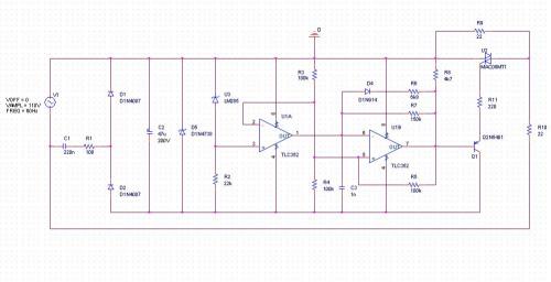
The mains voltage is modelled as a AC voltage supply. The circuit is powered directly from the mains via a capacitive divider, avoiding a large power resistor; this is possible due to the low power consumption of the dual comparator (MAX972 or TLC352) and the sensitive gate triac (with a gate current to fire of under 5mA).
When the circuit is powered on, the positive input of U1A is first biased at -2.5V. The triac is off and the current in the toroids is limited by R9 (you may want to adjust this value depending on the required power). The current through C1 and R1 is slowly charging C2 (not exceeding the 8.2V breakdown voltage of the zener diode D5). As soon as the supply voltage exceeds 5V (that is, the negative input of U1A is at -2.5V), the U1A output flips and triggers the oscillator built around U1B. This oscillator runs at about 10KHz and feeds (through Q1) current pulses in the gate of the triac. These pulses instantly fire the triac, however, the stored charge in the gate triac is to large to be evacuated in 100uS. The triac stays on forever, bypassing the current limiting resistor, until the mains power is shut down.
The delay is determined by the value of C1, R1 and C2. It also depends on the supply current required by the comparators. You may want to experiment a little to find the best values for these components, in particular if you decide for other comparators or have a different mains voltage.
Power on circuit
We would certainly like to implement some sort of standby mode for the amp, at least because the front panel is no place for a bulky, ugly plastic rocker switch to support 6-10 amps. We would like to control the power by the means of an elegant low power momentary switch pushbutton . This poses some delicate issues. First, the pushbutton momentary action has to be converted to toggle operation (with all the required contact debouncing). Secondly, this switch has to control the power supply CTRL input, described here and to allow further control expansion (e.g. for a backpanel remote control port used for chained operation with other audio system components).
These requirements are met by the schematic shown below (click on the image to get a high resolution version). The schematic is also included in the archive you may download here.
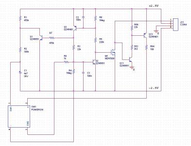
The button is a ring illuminated anti-vandal switch, manufactured by Bulgin. This pushbutton supports 50mA at the contacts while the 2400mCd green LED require 25mA. Q2 and Q3 are in a thyristor equivalent circuit. When the circuit is powered on, the thyristor is safely turned off (C2 and C3 are taking care of a consistent off startup state, avoiding accidental firing the equivalent thyristor by a high dV/dt in the circuit power supply). The CTRL output (the MOSFET drain) is low, disabling the +/-57V rails, C1 charges through R1 and R2. When the button is depressed, the charge accumulated in C1 is dumped in the base of Q2, turning on the thyristor. The CTRL output (the MOSFET drain) is activated, Q1 is saturated and C1 is relatively quickly discharged through R2 (the time constants associated with charging and discharging C1 are taking care of the required switch debouncing). When the switch is pressed again, C1 sinks the Q2 base current, the thyristor goes off and Q1 allows C1 to further charge.
The M1 MOSFET open drain is controlling the power supplies by OR wiring to the node (all outputs connected here are open collector/drain). Q4 and Q5 are feeding the switch LED.
A view of the PCB is shown below (click on the image to get a high resolution version). The Gerber files can be downloaded here. The switch is of the screw terminal type and installs directly on the PCB. The switch itself is attached through a 7/8" hole in the front panel.
Protection circuitry
A reliable amp has to protect itself against thermal effects and to signal and protect the speakers against oveload/clipping (a well known tweeter killer) and large output DC offsets.
These requirements are met by the schematic shown below (click on the image to get a high resolution version). The schematic is also included in the schematics archive you may download here. This circuit is common to both channels.
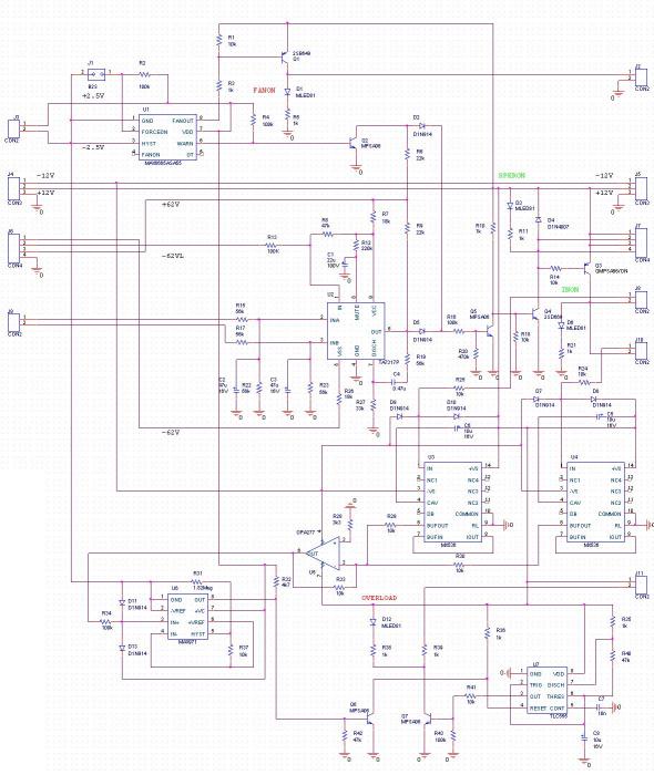
The thermal protection is provided by a MAX6665ASA55 circuit. This kind of protection is absolutely mandatory, in particular for this amp. We noticed that as soon as the output trannies case temperature reaches 100C (this is anyway a big no-no for power devices reability reasons) the amp may become unstable. MAX6665ASA55 has the temperature limit factory set to 55 degrees centigrades. As soon as the temparature exceeds 55C, the FANOUT output is activated. If the temperature further rises to 70C while the fan is on, the WARN output goes low, disconnecting the load through Q2 and the diode logic. The circuit is set for a hysteresis of 4C, avoiding a potential "relay chatting" condition. J1 is a jumper to force the fan on, something useful as a special configuration if the amp is going to work in a known as thermally harsh environment.
The output offset protection and de-thumping circuitry is build around a Toshiba TA7317P IC. This little circuit in SIL-9 package is very handy; it provides protection against a missing +/-57V rail, disconnects the speaker if the DC offset at the outputs is larger than a couple of volts, provides a 4 second delay in connecting the speakers and disconnects the speaker before the +/-57V power rails are dipping, to avoid the power off (by the backpanel switch, otherwise the power on circuitry presented above is taking care of this function as well) thumping. All of these for under $1!
The TA7317P circuitry is following closely the datasheet application. One not so obvious feature is the power off behaviour. Pin 1 is able to both source and sink current. If the current in Pin 1 is <-0.5mA the output is enabled, otherwise the load relays are disabled. At power off, the -57V auxiliary power supply described here drops fast (the 4.7uF filtering cap discharges very quickly) before the 20,000uF caps are fully discharged. This triggers a quick load disconnect, avoiding a potential loud thump when the amp is powered down via the backpanel switch.
A final note: the +57V supply for the TA7137P circuit has to be tapped before the power relays on the power supply board. This is to ensure the correct power on state; if both +/-57V rails are missing, the circuit output is floating and hence the output relays are activated which would be incorrect. If the +57V supply is present, the output relays are not connected until the -57V supplies are available and the 4 seconds delay time elapsed.
The circuit output energizes both the output relays (in parallel) and the front end on board reed relays (normally closed). This is to avoid any possible transient outputs during the power on sequence.
Care should be taken when selecting the output relays. A high current model with silver contacts is definitely recommended. We experimented with a number of relays and definitely some cheap models are introducing an inacceptable level of distortions due to improper contacts materials and/or mechanics.
The overload/clipping protection circuit is rather complex and it's functional requirements are defined by the clipping signal generated in the front end board. The clipping signal is bipolar, so it has to be rectified and filtered to a DC component. This is achieved in a MX536 precision rectifier circuit (one for each channel). You may have some problems sourcing these ICs, but they can easily be replaced with a high speed dual opamp and a few passives. The DC outputs are summed in an opamp and the output is fed in a MAX971 window comparator with hysteresis. When the comparators output flips, the 555 IC start oscillating at about 1Hz, signalling the overload condition on the front panel. The precision rectifiers and the comparator inputs are protected against overvoltages by diodes.
All conditions are monitored by on-board LEDs.
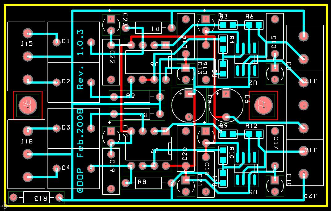
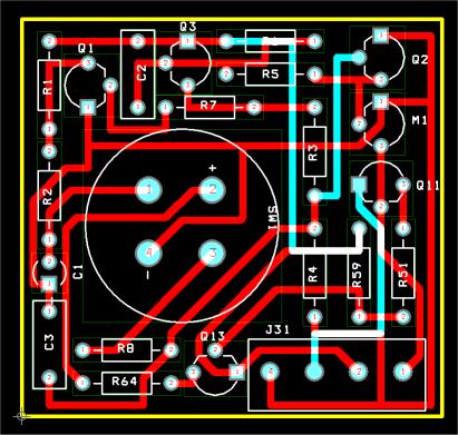
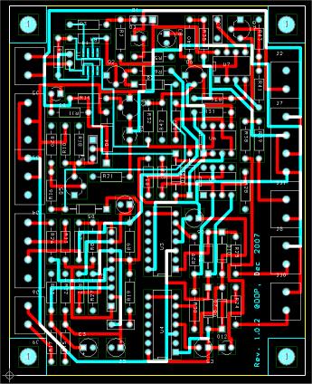
A view of the PCB with the top ground plane removed is shown below (click on the image to get a high resolution version). The Gerber files can be downloaded here.
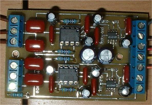
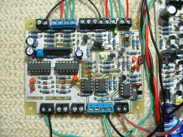
A view of the protection circuitry assembly is shown below (click on the image to get a high resolution version).
Balanced input circuitry
Unfortunately, because of the current architecture of the whole amp, it would be very difficult to build the amp input stage natively balanced. What's left is a balanced input to single ended converter - which is fairly simple (although not trivial to build, if it is to conserve the amp performance).
Such a converter can be buit either with discretes or around op amps. We experimented and evaluated three versions, the first based based on Bruno Putzey's differential amp published as Convention Paper 6294 at the 117th Convention 2004 October 2831 San Francisco, CA, with some improvements (output stage, servo, modified compensation, etc...), the second around a Burr Brown's OPA1632 high performance, fully-differential audio opamp, and the third in a buffered (LM4562) differential (OPA211) amp.
The OPA1632 had dissapointing performance in a single ended configuration. While the differential output performance was below our measurement resoultion, the single ended configuration THD20 was around 15ppm and the 19+20KHz CCIF IMD was at -97dB, all at 1KOhm load. A degradation in the single ended performance was expected, due to the lack of even harmonics cancelling, but the final results were no match for the single ended PGP amp performance.
The discrete design and the LM4562/OPA211 stages had comparable performance of around 0.7ppm THD20 and 19+20KHz IMD performance. We were unable to identify any advantage of a discrete design over the opamp, so, for cost and space reasons the winner was the buffer/differential opamp based amp. The schematic is shown below, the schematic is also included in the schematics archive you may download here.
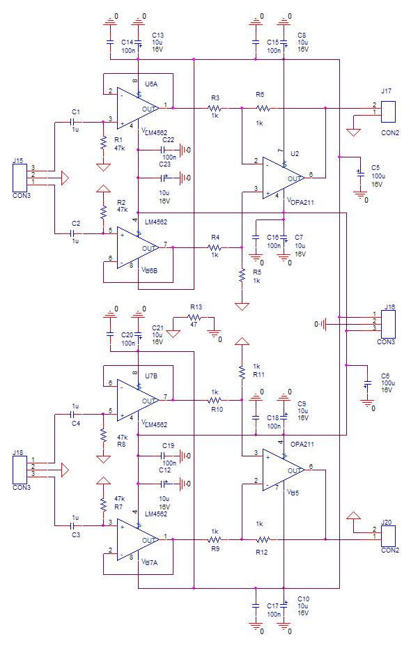
All power supply decoupling electrolytics except C5 and C6 are tantalum. To as much as possible conserve the CMRR, all 1KOhm resistors in the differential stages are 0.1% precision.
OPA211 has outstanding characteristics (see the TI datasheet here), being probably the best audio opamp on the market today. It though comes only in SOT8, so we decided to build the whole differential part using SMD parts and technology. We also experimented in both the buffer and the differential amp stage with OPA134, OPA627, LT1115, AD797 but only OPA211 made it for both the distortion AND the noise criteria. It is not a cheap opamp though, so our next preference would be AD797 for the differential stage and OPA2134 for the buffer.
A view of the PCB with the top ground plane (on the solder side) removed is shown below. The Gerber files can be downloaded here.
A board is shown below (it's an experimental version with aluminum electrolytics and OPA134 buffers)