The Front End
As for the EC OPS, all connections are done via terminal blocks. J1 and J6 are the positive and negative power supply conncections; it is recommended that you twist the power supply wire and the associated power ground wire together, so that the stray magnetic fields will have little impact. More details on wiring and grounding will be given in the Wiring the Beast section.
J2 is the input connection. Please note the signal ground that is connected to a power ground through a hum reduction resistor R16. The input signal is shorted by a normal close reed relay contact. This relay is energized (allowing the input signal to flow) by the auxiliary circuitry that is discussed in here on another page. The PCB is designed for a Hamlin HE721C1210 12V SPDT relay with integrated diode; for testing purposes only you may want to skip installing this relay until the whole amp construction (including the auxiliary circuitry) is completed.
The same signal ground is the reference for the feedback connection at J5.
J4 is the control terminal block. It inputs the signal (12V) required to energize the input relay and outputs the clipping indicator signal. Both are referenced to the power ground. The clipping indicator signal is shown here, the auxiliary circuitry is further processing this signal.
J3 is the output block terminal. It connects the front end to the EC OPS. Note that in the initial stages of the construction, after assembling the front end board, you may want to short the J3 connections and also connect this point to the feedback output at J5. This would allow you to measure the bias points in the front end, without connection the EC OPS. The circuit should be well DC balanced, while the output should be ideally at +/- a few millivolts. We build two front end boards; one has an offset of -1.2mV, the other is at 9mV These offset values are ending up across the speaker output terminals, so it is critical that you bring them as low as possible. The common reasons for large offsets are circuit assembling errors or mismatched components. We did not match the active parts as long as they came from the same tube, but we measured all metal film resistors and confirmed their values and tolerance of 1%.
No heatsinks are required on board. Q5, Q20 and Q46, Q31 the series regulators in the MPSU will be the warmest parts but nothing to worry about. Q3, Q13, Q19, Q22 and Q44, Q32, Q29, Q25 will also get a little warm.
If you cant source 2SC2240/2SA970 you may go ahead and replace them with 2N5551/2N5401 (they have a different pinout, so you may need to change the PCB layout). These transistors have higher noise but can do a fair job here. It is not recommended that you replace 2SC3503/2SA1381 (Mouser carries the Fairchild equivalents KSC3503/KSA1381 for pennies anyway) but mostly the VAS pair 2SC3601/2SA1470 with other so-called equivalents. This pair (made in Sanyo, having ICmax=150mA, VCEmax=200V, Cob=3pF and FT=400MHz) enables the ultimate performance in the VAS.
C4 is the DC blocking capacitor in the feedback loop. A 35V high quality non-polarized electrolytic is recommended here; lower voltage parts may have higher leakage currents. You will also note the input bootstrap circuit. This circuit raises the front end input impedance and is also responsible for the low frequency overshoot shown here. If you dont like the overshoot size you may reduce the C4 value to 220uF. If you are not bothered by a lower input impedance, you may eliminate the bootstrap circuit by making R54=100ohm and replacing R57 with a strap. C4 needs then to be 470uF, as the amp Fj has to be defined by the input cap C31.
C31 should be a high quality film capacitor (polycarbonate will do). If you find the 10uF part to bulky, you may replace it (as we did) with a 6.8uF/50V part. The impact on the low frequency characteristic will be minimal.
All capacitors under 1nF are ceramics NP0. Contrary to a wide belief that ceramic capacitors should be avoided in the signal path, we found absolutely no differences between ceramics and polycarbonate parts.
All caps over 1nF are polycarbonate or stacked metal film.
D3 and D12 protection diodes have to block almost the entire power supply voltage (here, +/-53V). Common small signal switching diodes (1N914, 1N4148) are supporting max 100V. This is the reason why we opted for the BAS21HT1 200V devices manufactured by Onsemi. These are SMD devices and are mounted on the PCB solder side (careful with the polarity of these little critters when installing!). Any other fast switching 200V diode will do here. As a last resort, you may sort 1N4148 parts, you may have a good chance to find 120V parts. If its not a SMD part, it can be anyway directly soldered on the solder side of the PCB.
Do not replace the LM329 6.9V references with equivalent Zener diodes. While from a DC perspective this may work, Zeners are very noisy devices. You will find that using Zeners will dramatically impact the S/N ratio of the whole amp.
All resistors are 1% 0.25W metal film, except for R49 and R40 which are at least 0.5W. If space for 0.5W parts is an issue, you may install for each 3x8.2K stacked (in parallel).
The front end requires little to none adjustments. If the parts are ok and properly installed the front end should work stable right away. While shorting the outputs and the feedback connection will allow you to measure the DC bias currents and voltage balance, you can not do full AC measurements. This is because the feedback network loads the output and at output levels over 10-15V the VAS stage will be current starved, leading to unacceptable distortions. The C9 and C24 capacitors should be chosen as the lowest value that keeps the amp stable under all circumstances.
The front end gain is set to 28. Changing the overall gain involves much more than changing the R49 resistor value. All internal feedback loops have to be rebalanced, so if you really need another gain value contact us for the details.
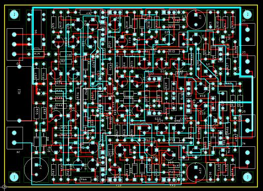
Click on the picture below to get a full image of the front end PCB (ground plane is removed). You may download the Gerber files here. It is a rather complex and dense board that requires some good soldering skills.
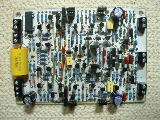
Click on the image below to get the full picture of a fully assembled front end PCB.
The front-end design is build around two concepts: the Comon Mode Control Loop (CMCL) and a modified version of prof. E.M. Chery's Nested Differentiating Feedback Loops (NDFL).
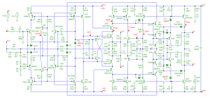
Click on the image below to get the Front End PCB schematic. You can download all schematics here.
Click on the images below to get the a large view of the front end full electrical schematic.
In the early eighties, prof. Edward. M. Cherry invented the technique of NDFL (U.S. Patent 4243943). Despite its simplicity, the improvement in terms of distortion reduction is of an order of magnitude. Amazingly, this technique was never widespread used in audio amplifiers. One reason could be that he confused the readers of his original paper cited here by combining NDFL with a two other tricks: enclosing the output stage in the Miller compensation loop (OMC) and (for unclear reasons and/or based on claims not entirely proven) using the signal at a tap on the Zobel network for global feedback. Not everyone was charmed by this magic... Another reason might be the poor clipping and recovery properties and, admittedly, solving this issue is not an easy task. We were able to tackle this problem adequately, probably a first in history of audio engineering.
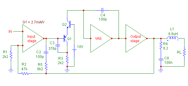
Cherry's original implementation (shown in the picture below) can be converted to a more commonly topology, that is, just a pure resistive divider for global feedback).
Prof. Cherry's approach was to make this system phase linear, even if this comes at the cost of a 14% oveshoot. Our approach was different and we choosed to keep the 2nd order system critically dampened, that is, no overshoot (the pulse responses are shown here).
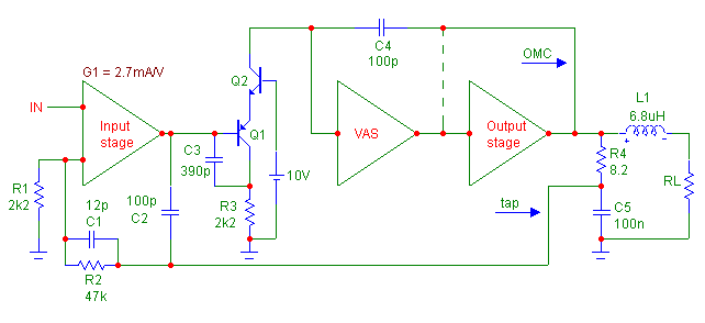
Now, if it is to remove the Zobel tap and revert to the traditional Miller compensation, while still keeping the 2nd order system critically dampened then the equivalent modified circuit would look like in the following picture.
It should be noted that the amount of overshoot is mainly influenced by a mismatch of the time-constants of C2 and R5 respectively C3 and R3, while C4 and G1 have a strong impact on the rise and fall times. The Q1 and Q2 configuration is derived from the so called high speed Rush amp.
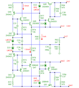
Of course, many other implementations are possible. Long story short, the topology currently used in our front end is depicted in the next picture.
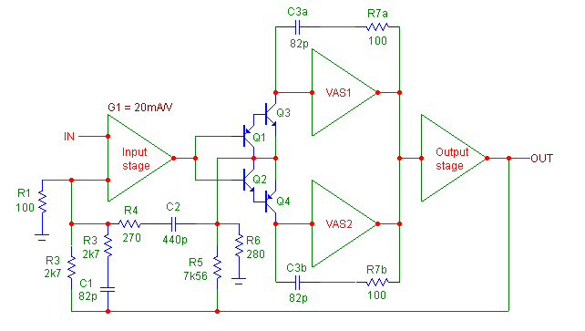
This one differs not only in that it is fully symmetrical, but also the feedback paths have been changed. Now the lag compensation (C2 and R4) is applied between the emitters of Q3 and Q4 and the inverting input of the preceding stage. Also, the nested feedback (C2 and R5 in the previous modified design schematic above) has moved to the inverting input (C1 and R3). Strictly spoken, this isnt any longer a nested feedback, as it leads to the same input as used by the global feedback (R3). Nevertheless, the behaviour of this topology is equal to the previous modified circuit. An important feature of this arrangement is the low requirement of drive current of the input stage.
The design rules for this case are completely different, for example the gain of the global feedback loop (around R3) is almost independent of the trans-conductance of the input stage.
The Ultimate Audio Amp
From Genesis to Revelation