From Genesis to Revelation
Yet Another Poweramp
Another way to skin the cat
The YAP Output Stage

YAP 3.2 was built in a modular fashion, with the output power stage (including the thermally compensated bias spreader and the overload protection circuitry) on a separate board. The front end goes on a separate board, attached to the heatsink.
The first question I had to answer was about the best output bipolar power devices. There are many wideband (Ft>30MHz) bipolar power devices available today; they all have about the same electrical parameters, however they may have significantly different Safety Operating Areas (SOA). A smaller SOA maps to the requirement to use more output devices for the same output power level. Also the SOA impacts the overall thermal budget and the overload protection circuitry design.
From a SOA perspective, the OnSemi MJL1302/MJL3281 are probably the best 30MHz devices. They also come in the TO-247 large plastic case, which makes them a little more efficient in the heat transfer, compared to the standard TO3 plastic case. The runner up was the 2SC5200/2SA1943 pair. This pair has similar electrical parameters, being only marginally worse in SOA. As a big plus, 2SC5200/2SA1943 is probably the cheapest pair around, being manufactured (as a second US source) by Fairchild.
But then OnSemi included a diode in the MJL1302/3281 case and created the ThermalTrak devices. Under the NJL1302/NJL3281 code lies a MJL1302/MJL3281 pair each with a diode on the same metal chip frame. While the diode is not on the chip, it is tightly thermally coupled with the power chips, which offers some nice features for building a thermally compensated output stage. The idea is not only to provide an "average" zero tempco bias source for the output devices, but also to make, as much as possible, the bias to follow the thermal variations of the power chips. This helps with reducing the distortions at low frequencies, but also to to avoid current starving the output stage, after a short surge in the power dissipation.
Bob Cordell has a throughout discussion on the ThermalTrak devices in his latest book; he also describes a few possible bias circuits that include the ThermalTrack diodes. The bottom line is that, while certainly useful, the ThermalTrak diodes are not very easy to use. They match the power devices Vbe tempco at about 25mA forward current, which is certainly outside a reasonable VAS bias current range. But then at 25mA forward current, the diode forward voltage drop is larger than the power devices Vbe, for a collector bias current of, say 100mA therefore, if used straight across the Vbe junctions, the output stage would be grossly overbiased at the zero differential tempco point.
From this perspective, the Sanken thermally compensated power devices are much better; they use on chip Schottky diodes to almost ideally match the tempcos and the forward voltage drops. But the Sanken devices availability, pricing, and the lack of a US second source, makes these devices a togh sell.
Let's take a look at the OPS bias scheme used in YAP 3.2. This bias scheme was originally developed by Sansui and eventually adapted for ThermalTrak devices by Bob Cordell.
What is the advantage of this bias scheme? To find out, recall the "standard" Locanthi T output stage. The most annoying problem with this circuit is the presence of the "acceleration" capacitor across the Vbe junctions of the OPS power devices. This capacitor is (as also shown by Doug Self) required for providing a base current path during the off switching process. That is, when one of the OPS halves switches off, the cap provides a current path for the base current, so that the base stored charge is quickly evacuated. Without such a current path, the bipolar power device off switching process is awfully slow, resulting in lots of crossover distortions. However, it is easy to overdo these capacitors; if they are to large, they trend to reverse bias the BE junction, even when the OPS half is turning on. As a result, again more crossover distortions.
Ideally, the OPS power devices should have an as close as possible to zero source impedance. You would note that D3, D27 and R250 are as close as possible to this ideal situation. D27 and D31, although being ThermalTrack on chip diodes, do not provide the required thermal compenstation. They only mirror the voltage across the thermal compensation diodes D29, D30, D33 and D34 (after substracting two non-thermally coupled forward drops of D35 and D36). Such an arrangement allows both increasing the equivalent tempco of the on- chip ThermalTrak diode chain, and also bringing the forward drop to the values required for the output stage to be biased at the optimum Barny Oliver point (26mV across the emitter resistors). The DC bias control loop is closed through Q63 and Q65. In practice, some speed-up cap is still required (reverse biasing the BE junctions accelerates the stored charge evacuation) but small enough so that the turn on impact described above can be safely neglected.
A little SOA calculation reveals that four pairs of ThermalTrak power devices are able to sustain 400W RMS into 4ohm and to provide the required margin for 2ohm transient overloads. If you decide for 2SC5200/2SA1943, then five pairs would be required. The heatsink has to have a thermal resistance Rth < 0.5C/W, otherwise the power dissipation temperature derating is the limiting factor.
As you can see from the above schematic, the YAP 3.2 output stage is, from an AC perspective, a bipolar triple. Some authors are praising the bipolar triple as the best thing since sliced bread. Others (including Doug Self) not so much - they dearly warn about potential stability issues in a high current gain configuration as the triple.
You need to see it by yourself to understand the destructive potential of a high power triple stability problem. The net effect of instability is a massive crossconduction of the OPS, then the OPS (transistors, emitter resistors, PCB traces) literally explode in a burst of light and smoke. After being biten myself several times, I decided to take a closer look at the triple stability. But how?
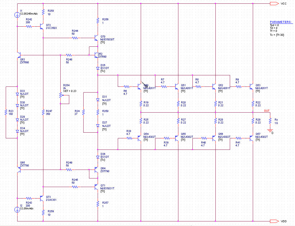
The triple stability problem can be reduced to an emitter follower stability analysis. Looking at the emitter follower as a current feedback stage, it is not obvious how this local current loop stability can be analyzed. There is no way to break the loop in a standard way, since the loop is internal to the active bipolar device (it is actually Rb'e that defines the loop gain, which in turn it's bias and Beta dependent). An entire thread was dedicated to the emitter follower stability, so I'll save here a long theoretical discussion and show the results only. But first, we need to define the OPS schematic, including the parasitic elements (capacitors ESL and ESR and PCB traces inductances). The resulting schematic shown below, the parasitic elements are the best estimates for the parts used (from the data sheets), the PCB elements (from the layout used to build this OPS) and the PS wiring properties.
The formulas required to plot the loop gain and phase are on the schematic; You can use these formulas to estimate the stabilty for other triple configurations and I would recommend using the second group (with Vx and Vy) because they return the correct phase polarity - otherwise, the results should be identical using both formula groups.
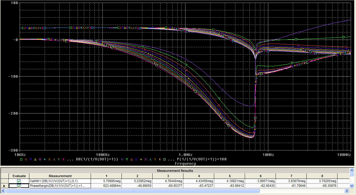
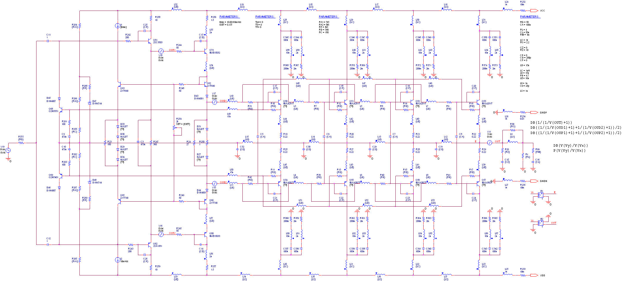
Here are some results, and unfortunately they are not pretty, but rather depressing. Assuming a pure resistive 4ohm load in parallel with a load capacitance of 0...100nF in 10nF steps), no output Zobel cell (RZ=CZ=0), no output inductor (L0=0), and all the parasitics defined on the schematic above, the triple overall loop gain is depicted below:
For any load capacitance other than zero, the triple OPS is not stable. Note the LF "loop gain" that is here actually the output device Beta.
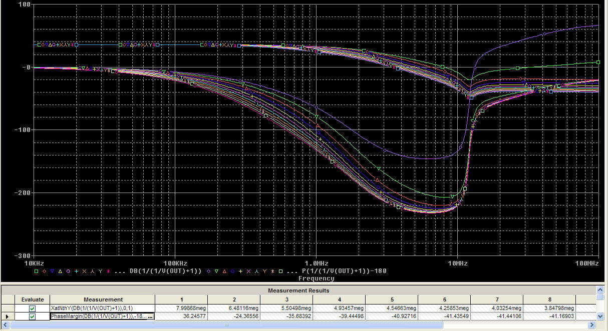
But remember, this is at 0V (zero volts) DC output. If we repeat the same for the output at 50V DC (which emulates the transient stability of the OPS) the results are much worse
The OPS is unstable even at zero capacitive load. This confirms what happens in practice. Power up the OPS, and everything seems to be fine so far. Increase the input signal so the output approaches the rail voltage, and the OPS starts to oscillate wildly. The reason for this behaviour is the output devices Cbc which increases significantly as Vbc approaches zero.
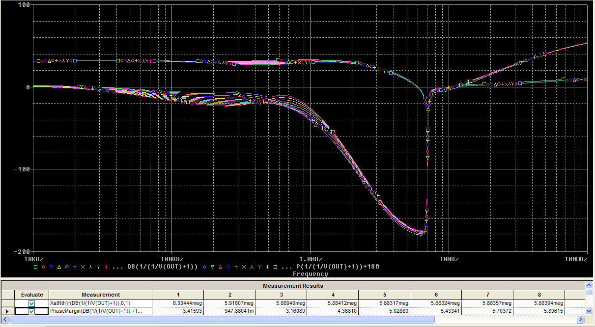
Even if we add the isolation networks (L0=1uH, R0=2.2ohm, CZ=100n, RZ=10ohm) the triple OPS still doesn't have enough stability margin for any practical purposes.
Now, what to do? By looking at the triple as a three stage amplifier, each with local feedback, we recall that it's always the middle stage that defines the overall bandwidth. That's because the middle stage "sees" at the output the relative high impedance of the last follower, therefore any capacitance would have a maximum effect on bandwidth. On the other side, the first follower would still isolate the VAS from the increased capacitive load.
'
So we need to add a fixed cap across the driver BC junction. The value of this cap is in the 100's of pF. That may look quite large, but consider the pre-driver output impedance (very low, it's still an emitter follower!) and the input impedance of the output stage (really, not that high, because the output devices are running at a relative high bias current, 100mA or so).
Now putting it all together, with a CD=470pF, the results are much better, the triple OPS is unconditionally stable even in the worst case capacitive load (which is around CL=50nF)
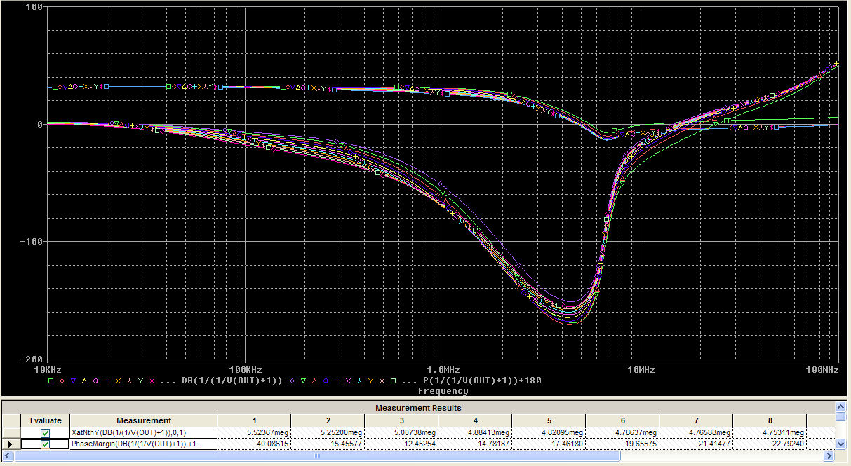
While the OPS overall bandwidth is around 5MHz (far up enough to allow pole separation at a global amp ULGF of 1MHz) the worst case phase margin is 12 degrees. That's good enough, we don't really need to provide the same phase margin as for the global feedback loop. In a sense, the situation is similar to the local Miller loop stability criteria, we don't need to provide 80 degrees of phase margin at the Miller loop ULGF of (e.g.) 30MHz.
After this lenghty (but I hope useful) discussion on the triple stability we conclude that indeed, the triple OPS may have significant stability issues, in particular if high speed devices are used (like having Ft=30MHz). Slower devices with Ft=4MHz have much less stability issues, but they would not allow high performance due to the limited global feedback loop gain they would allow. I also hope the role of the isolation networks (output coil and Zobel) in providing OPS stability is also better understood. A good example of transient instability was also presented. When the OPS output approaches the supply rails, the OPS phase margin quickly degrades. This is a problem that plagues, to a more or less extent, many audio power amplifiers, in particular when driving difficult capacitive loads, as electrostatic speakers.
The bottom line is that deciding for a triple bipolar output stage, built around high speed devices, needs a careful design (including PCB layout) and analysis (including the device and PCB parasitics). Using a fixed cap across the BC junction of the drivers is a good solution for stabilizing a triple OPS.
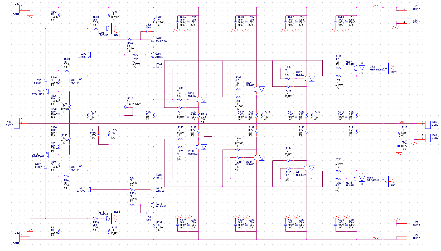
This being said, here's the board level schematic of the YAP3.2 OPS. It contains a few changes compared to the generic schematic previously shown, and also the dual slope overload/overcurrent protection.
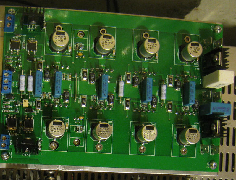
A good friend of mine commented about the board schematic missing the base-collector driver fixed caps discussed above. Reason was, these caps are not on the PCB layout, but rather soldered directly on the MJE 15032/33 through-hole BC terminals (see the photo of the assembled board below, the caps are the small yellow-mustard parts). I have now added these caps on the schematic below (C225/C226) but don't look after them in the PCB layout available for download.
The OPS was implemented in SMD technology, using 1206 parts. The emitter 0.22ohm resistors are also SMD, 1W, these are much better than the wirewound (and usually inductive) regular through hole resistors. The power devices and the drivers are mounted on the bottom side and bolted to the heatsink through the PCB holes, that's the best way to keep the parasitic PCB elements low. FASTON connectors are provided for the power supply wiring. The board schematic shows the acceleration caps as 0.47uF, this is in fact much larger than required. I am currently running this OPS with 22nF each caps (so a total of under 100nF).
The dual slope overload protection senses the current through the output devices and approximates (by using a Zener voltage controlled break point) the SOA curve by two segments. This allows avoiding triggering the protection at levels that are well below the SOA (for low Vce). Using the R235/C223 network, the protection is also set to filter out very short transients. R210 adjusts the optimum bias current, which was found slightly over the Oliver point, at about 29mV across the 0.22ohm emitter resistors. As you can see, one pair of ThermalTrak diodes is not used. The 1uH output inductor is not on the PCB board. Due to size and radiated mag field it is installed (together with the parallel 2.2ohm/20W power resistor) close to the speaker connectors.
The temperature stability is excellent, at a 90 degrees heatsink temperature the output stage bias decreases with less than 3% compared to the bias point set at 25 degrees.
You can download the OPS PCB Gerber files.
Here's a picture of the assembled (and bolted on a 0.5 C/W heatsink) OPS board. See the YAP Measurements section for experimental results.