HPS 1.0 was nothing more than an incarnation of Dennis Colin "LP 797 Ultra-Low Distortion Phono Preamp" published in AudioExpress. The original article is available here (scroll down the list and watch the two important corrections). I liked the idea of distributed active RIAA correction and also the concept of using negative feedback to linearize the input stage.
Now, the original Collin design has a few significant flaws (openly admitted by the author in the same article), one of them being the very poor PSRR in the input stage. To avoid hum and other noise artifacts to enter the signal chain, this design calls for a solid power supply, much better than the original. So I decided to add a Jung regulator on the same board. The plan was to feed HPS 1.0 from a 24V wall wart, so some extra circuitry is required to split the power supply. I decided for a TLE2426 rail splitter. This little circuit works great and it's ideal for balanced rails current; any imbalance flows straight through the virtual ground created by this circuit, so I would advise to be careful in your applications. The HPS 1.0 currents are already imbalanced by the input stage JFETs, dragging current from the positive supply only. The TLE2426 gets a little hot, but nothing to worry about. However, further extending the same concept to more paralleled JFETs may create some serious power dissipation issues.
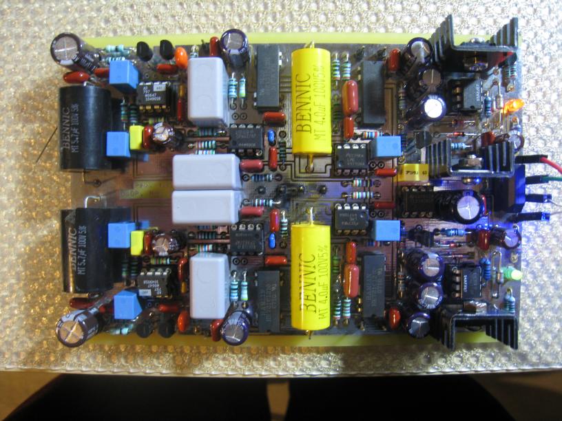
The entire construction fits (and the PCB is designed accordingly) in a standard extruded aluminum case like this. You can get such a case from your distributor of choice (Digikey, Farnell, Mouser, they all carry the Hammond products).
There's not much to tell about construction; just use good quality components (polypropylene caps, metal film resistors) and low noise opamps (AD797 or LT1115, LT1128, LME49710, OPA211 on a SMD adaptor) and the good results are guaranteed. The relays are DIP case 12V models. It is a good idea to mute the preamps before powering up/down or switching the gain to avoid a large thump into the speakers.
For this build, the dynamic range (aka the headroom) is around 22dB at 1KHz, for the max gain of 64dB and +/-17V supplies. This is not bad, but has a certain audible as you'll find later on this page.
As you will find in the Measurement sections, the equivalent input noise of this construction is about 0.9nV/rtHz. This is very good for a MM cartridge (the NAD PP3 preamp has 8nV/rtHz for the MM input) but not that great for MC. The hiss is clearly audible, on the 64dB gain setting, even in not very sensitive speakers. Therefore, even if it has the required gain, I cannot recommend this construction for low output MC cartridges; you may want to look at the HPS 2.0 below for that.
Although the Jung regulator helps in reducing the hum and noise artifacts injection in the input stage, some residuals (captured from the supply input wiring and the ambient, the case is aluminum) are still slightly audible; again, refer to HPS 2.0 for a low output MC cartridge.
HPS 2.0 was designed and implemented having in view the above issues. Some important differences to the original Dennis Colin design are implemented:
- HPS 2.0 uses 4 2SK170 low noise JFETs in the input stage. The equivalent input noise of the input stage is inversely proportional to the square of the number of paralleled input devices; it is therefore expected, theoretically, HPS 2.0 to have half the noise of a single 2SK170 input stage (1-1.2nV/rtHz) plus the contribution of the source resistor (10ohm, 0.4nV/rtHz).
- To increase the PSRR, the input stage was cascoded.
- To further improve the hum and noise injection in the input stage, a local power supply was added.
- A dedicated power supply (to replace the wall wart and the TLE2426 rail splitter) was added as well. To keep hum to a minimum, this supply was designed as a separate unit.
- A switchable input impedance (Rin, Cin) to add some extra flexibility.
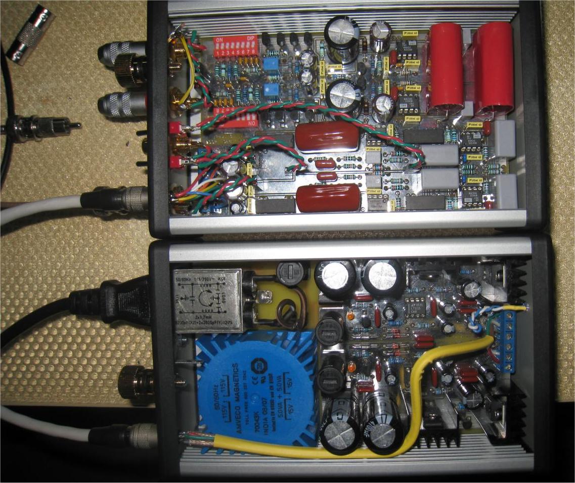
Both PCBs will fit each in the same extruded aluminum case as for HPS 1.0. Two 5 pin connectors and an appropiate cable are required to connect the power supply to the preamp.
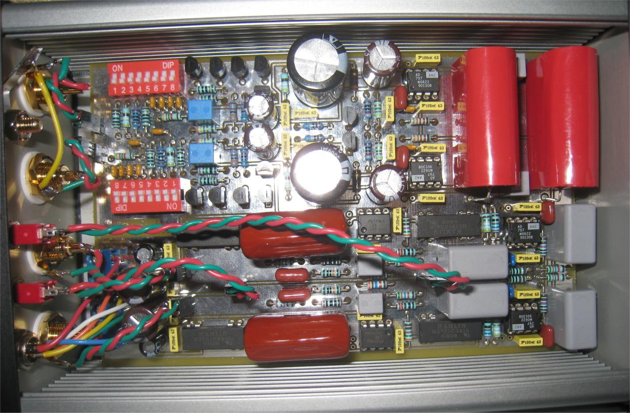
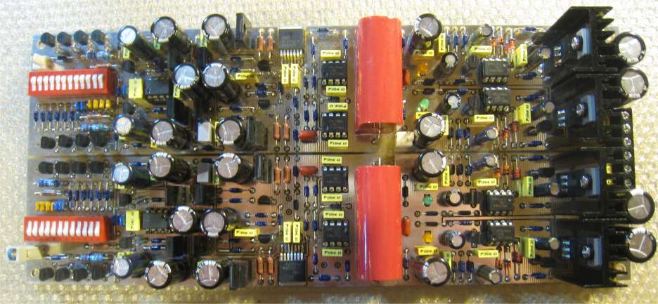
Here's a picture of the HPS 2.0 signal board.
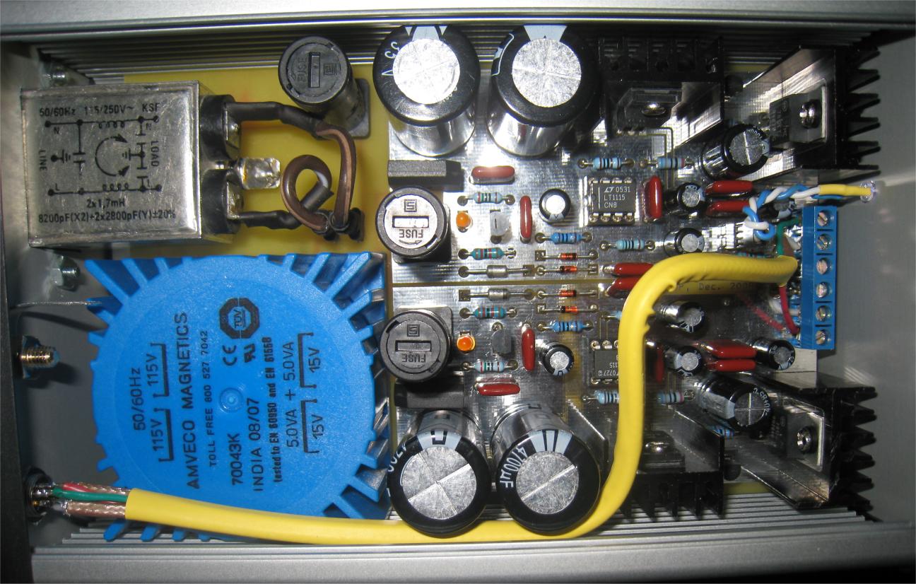
And the HPS 2.0 power supply board
Linked together...
The same construction details as for HPS 1.0 apply. HPS 2.0 has the same gain, the same dynamic range as HPS 1.0 but a much improved noise performance. As you will find in the Measurements secton, the equivalent input noise is around 0.6-0.7nV/rtHz; it can be therefore successfully used with MC cartridges down to 0.5-0.7mV output at 5cm/sec.
The only criticism I was able to hear about HPS 1.0 and 2.0 (beyond the regular grumbles from the anti-feedback crowd) was related to the significant number of caps in the signal path. Even if these are all high quality film (polypropylene) types, it would nice to build a preamp with no caps in the signal path (except the optional output cap). The headroom of only 22dB was also under fire, claims that only tubes can provide a large enough headroom, and that a minimum of 32dB is required anyway to allow through the vinyl "pops".
HPS 2.0 is still no match for the Vendetta Research and the Pass XONO, when it comes to noise performance. I had the opportunity to reverse engineer both models and I can tell there's nothing very special about these performances, beyond some unobtanium Toshiba JFETs (Vendetta) and some very good practices in wiring and grounding (both models).
Can an experienced DIYer beat the lowest noise phono preamps ever built commercially, at the same time avoiding to spend several good thousands of dollars on such? The response to this question is within HPS 3.1.
To beat the 0.4nV/rtHz noise, we have to abandon the Colin architecture; not only is the 10 ohm source resistor eating up the entire noise room (it already has 0.4nV/rtHz Johnson noise by itself) and going down would require much larger RIAA caps in the input stage, but also directly paralleling more than 4x2SK170 is not practically feasible. Feedback or not, the input stage becomes unstable.
HPS 3.1 addreeses all these issues and is perhaps the best RIAA preamp ever built. Here's a synopsis, measured on a finished prototype actually running in my system:
- 0.35nV/rtHz equivalent input noise (and this is with 2SK170BL/2SJ74BL JFETs straight from the tube, no matching or sorting was done; a prototype with sorted parts showed measured noise down to 0.28nV/rtHz)
- 0.001% total distortion 20Hz-20KHz
- 0.002% IMD distortions 20Hz-20KHz
- +/-0.1dB RIAA matching
- better than -130dB cross talk
- +/- 22V power supplies, allowing a 32dB dynamic range/headroom. The preamp clips at 20mV input, for a gain of 60dB @1KHz
- 50uV output harmonic noise (mostly 60Hz and 20dB less 3rd harmonic at 180Hz), the equivalent of 5nV harmonic noise voltage at input.
- Zero caps in the signal path (except for the optional cap at the preamp output). Less than 10mV offset before the output cap (the equivalent of 1uV input offset, gain at DC is 80dB.
- Dual mono architecture, completely separate signal paths, power supplies and mains transformers.
The HPS 3.1 architecture is built around the headamp concept. The low noise input stage is now a pre-preamp with a flat frequency response, set at a gain of 32dB, that feeds the distributed RIAA active stages (built around low noise opamps). After much consideration I decided that such a construction should not include any MC/MM gain switching and that a gain of 60dB is all one would need, even for the lowest MC cartridges like the Ortophon. 60dB gain would feed the standard 200mV output to a preamp for a 0.2mV input. Anyways, if more gain is required, it is not a big deal to recalculate the passive networks around the opamp stages.
I already mentioned that one can hardly add more than four parallel JFETs to the Colin architecture without risking to get a nice and expensive 100MHz and up oscillator. Adding gate resistors would stop the oscillations, but would also add to the noise. So a new architecture is required; take a look at the headamp schematic.
Four 2SK170BL/2SK74BL each are paralleled in a symetrical configuration. Each branch is cascoded by Q3/Q4 (great care was taken here to avoid any noise injection from the cascode fixed supply, a low noise LM329, extra decoupled for a very low corner frequency). A folded cascode stage follows and the current is converted to an output voltage by a high voltage, JFET input, OPA552 opamp. It is interesting to remark that in such a configuration it is essentially the noise current that would affect the output noise; the input voltage noise is effectively shorted by the low impedance at the opamp inverting input.
At the same current node, a lead-lag frequency compensation (R17/C16) is provided to set the unity gain frequency at about 1MHz. This, in combination with the lag compensation provided by C13, provides a phase margin of about 80 degs. The open loop gain is independent to R2/R23 (the input stage load) being essentialy Gm*R16 where Gm is the JFET stage transconductance, or about 8*2*Id/Vt where Id is the drain current and Vt is the JFET pinch voltage. As long as the input stage gain is larger than 1/3 the total gain (set here at 40 by the feedback network) the R2/R23 impact on the output noise can be safely neglected.
This configuration allows a very small source resistor (here it's the equivalent of 0.5ohm, in the final design it is 1.1ohm) but requires in turn a pretty high output current, to feed the feedback network. Hence the selection of OPA552, having a maximum output current of 200mA.
One disadvantage of using a flat fixed gain pre-preamp is that this stage defines the high frequency headroom. While at high frequency the RIAA stages have low gain, it is the front end that limits the output swing, and the limitation is in the ability of the opamp to drive the low impedance feedback network. After mucho calculations and experimenting (and here's where HPS 3.0 was buried, if you wondered about) I determined that the input stage needs a 8V swing to conserve the low frequency headroom of 32dB (that is, a +/-20V swing at the preamp output) defined by the output stage opamp. Which in turn leads to a feedback network impedance of 40ohm and an equivalent source resistor of 1ohm.
The headamp employs a servo, keeping the DC at the output to under 50uV. A good low noise JFET input opamp should be used here. The servo acts by adding/substracting current from the folded cascode stage and fortunately, due to the relative independence of the output noise to the R2/R23 impedance, this barely affects the total noise as well.
A 12 positions DIP switch is now used to switch the input impedance (6 resistors 10, 50, 100, 200, 500, 1k and 6 C0G ceramic caps (yes, I can already hear the grumbles, trust me, they are excellent) 22, 47, 100, 220, 330, 470pF). With the DIP switches all off, the input impedance defaults to 47k/0pF.
The folded cascode fixed voltage is provided by a LM431 parallel regulator. These critters are not famous for low noise, but R208 and C203/C204 are filtering the noise to a negligible level. R208 also does the job of avoiding loading the LM431 output vith a capacitive load, which may lead to oscillations.
OPA552 may look like an exotic component, in fact it is not. It's a high voltage/high current, high speed, JFET input opamp, coming in TO220, in full production from TI. You can get them from your distributor of choice, for under $10. It's rather difficult to recommend a replacement, though. The only other combination that I have experimented with, to replace the OPA522, was a regular JFET input low noise opamp (OPA637, OPA827, OPA134) followed by a nigh voltage unity gain buffer like the National LME49600. Set aside the extra complexity, such a combination ends up bing more expensive; the LME49600 costs well over $10. Finally, you may settle for a low voltage high current JFET input opamp of your choice, but this will affect the overall headroom.
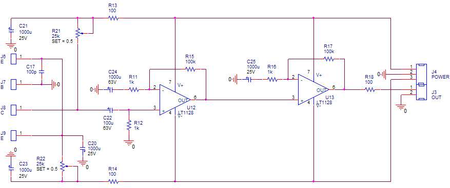
The two following stages are performing the distributed RIAA active correction and providing the extra gain up to 60dB at 1KHz. R207 and C215 adds the extra 50KHz pole.
R202/R240 and R213/R226 should be 1W/50ppm metal film or metal foil resistors. The number of electrolytic caps is pretty large, but none of them is really in the signal path; they all have decoupling roles. Any good quality models can be used, I am personally like the Panasonic 105 degs/3000 hours series.
You don't need to match or sort the JFETs. It doesn't matter for noise anyway and the servo takes care of the offset. You need the BL series (6...12mA Idss) but any parts straight from the tubes will do just fine.
The HPS 3.1 power supply is located on the same board and is the same Jung regulator but series regulators are now power MOSFETs. You can replace them with any darlingtons in TO 220 without any other changes. Also, to increase to open loop gain, the current sources vere defined using a pair of high voltage JFETs. They don't need to be in particular of very low noise, essentially any 50V JFETs will do. You can of course replace them with resistors as in the original Jung schematic, with a slight penalty in the output impedance. Here's the HPS 3.0 power supply board level schematic.
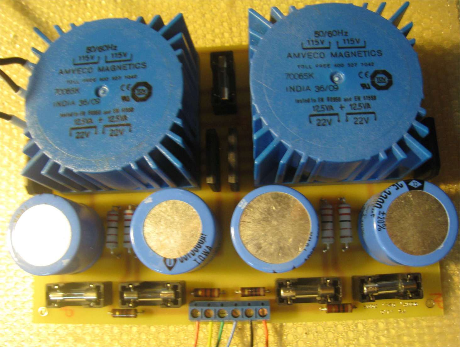
The mains transformers (Amveco toroids, 2 x 22Vac, one for each channels, the rectifier bridges, the fuses and the main filtering caps are placed on a separate board. I chosed to save and build this board on veroboard; you may choose to do an inhouse single sided PCB. Here's the mains power board schematic.
This board also holds the antiparallel diodes (a pair for each channel) designed to break the ground loop; 1N4007 are good enough here, for a high power amp you may want to use a large rectifier bridge for the same function.
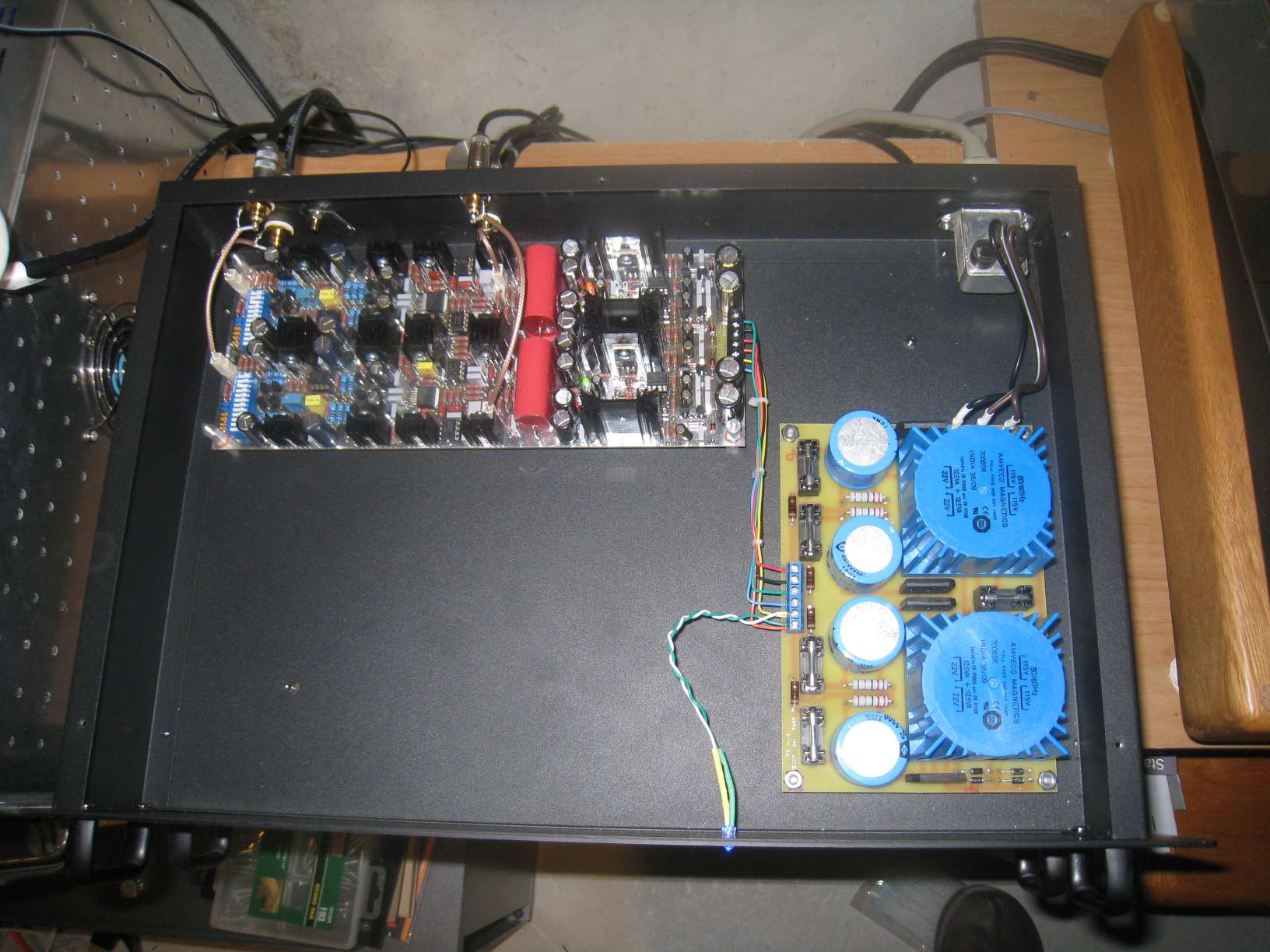
The left and right channels grounds are connected together with a strap, at a single point close to the input, on the main board. This is not a ground loop, as nothing is returned through this link.
Finally, the wiring of the whole construction is as usual a critical step. You may want to follow the schematic here. This method provided a harmonic noise of less than 50uV at the output, mostly 60Hz and some -20dB 3rd harmonic at 180Hz. This is completely inaudible in the speakers, even if they are 96dB efficient as my horns.
That's about it, for the moment. I would only like to add that although all these constructions are "plug and play" (that is, they work straight out without any adjustment required) they are not simple construction. In particular if you want the ultimate performance of HPS 3.1 you have to be very careful with the construction details, in particular the wiring.
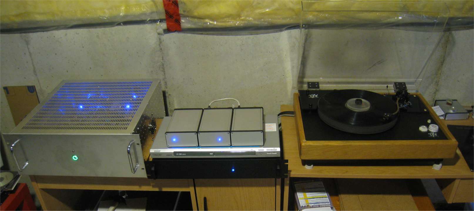
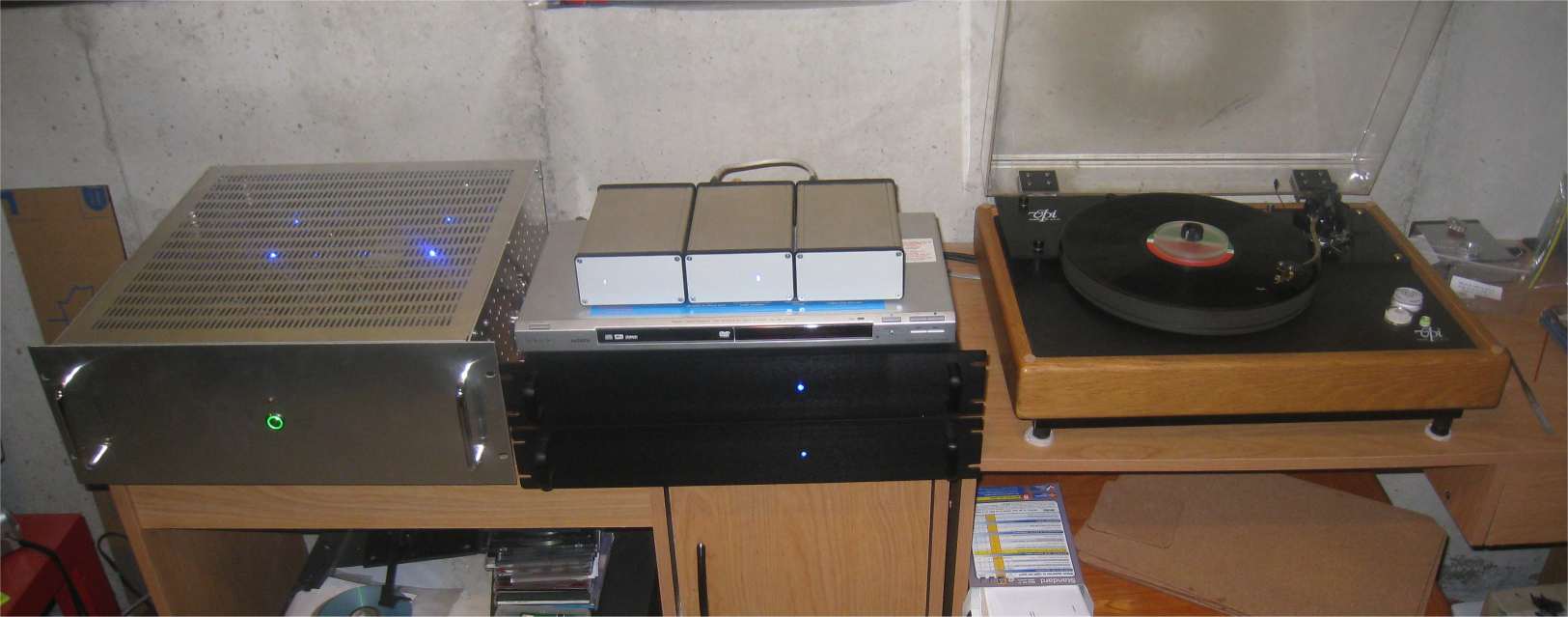
And a picture with the whole setup, during the listening tests. Left, the PGP amp, middle top left, HPS 1.0, middle top right (in two cases linked together) HPS 2.0, middle in between a CD player, middle bottom (in black) HPS 3.1, right VPI TT.
HPS 4.1 was intended as a new approach in the head amp. While they are ideal for high input impedance low noise stages, JFETs have certain issues.
- Complementary low noise JFETs are now almost extinct.
- Their large nonlinear input capacitance (Ciss) is a problem when paralleling devices, a source of distortions that is not included in the feedback loop.
- It is also not easy to achieve high gain in the input stage, more than 1/3 the closed loop gain, to make the S/N independent on the second gain stage.
Complementary low noise bipolars are still available, even as NOS devices or devices that are, due to the manufacturing process, inherently low noise, having very low Rbb' (notably the Sanyo FBET process devices). The BJT equivalent voltage noise is essentially determined by the base spreading resistance Rbb' plus a component inversely proportional to the square root of the collector current, while the equivalent current noise depends on the square root of the base current. The BJT equivalent current noise can't be neglected, in particular for high impedance sources; a noise optimum (or compromise) exists, where Ic=Vt*SQRT(Beta)/Rsource. As a rule, if the source impedance is low (as for the moving coil cartridges), it is a good idea to run the low noise bipolar gain stages hot, as this would leave only the Rbb' as a noise source.
Here are some Rbb' measurements I did:
Model
Beta
Vno [nV/rtHz]
Vni [nV/rtHz]
Rbb'
2N5551
131
470.4
1.41
104.5
2N5210
350
668
2.01
227.9
2SC2909
155
490.8
1.47
115.4
2SC2362
188
518
1.55
130.5
2SC2240
174
322.4
0.96
41.5
MJE15030
88
216.13
0.63
10.1
KSC3503
107
245.7
0.72
17.6
2SC3601
135
178.1
0.51
1.9
2SC2547
274
176.8
0.51
1.7
It is obvious that many so-called "low noise devices" are not really low noise. In particular, the 2SC2240 and 2SC2909 are dissapointing. However, some medium power devices (MJE15030), the Sanyo FBET devices (like the 2SC3601 and the lower current 2SC3504) and of course the special designed low noise device (like the Hitachi 2SC2547 and the ROHM 2SD786) are doing great. Usually the pnp in the complementary pair has lower noise, so measuring the npn device is mormally good enough. Here's the test jig for measuring Rbb':
Feed the jig at +/-15V. Set the collector current using R22 and the collector voltage by R21. Calculate the total gain (101^2 *(Ic / 0.026) * R12) and measure the output noise in nV/rtHz. Then calculate Rbb'.
HPS 4.1 follows the same head amp and distributed RIAA correction architecture as HPS 3.1. In fact, it is only the head amp that is heavily modified to adapt to the new requirements.
A head amp is a very low noise, wideband and as much as possible linear amplifier that connect between the MC or MM cartridge and the RIAA correction circuitry. For all purposes, the head amp sets the overall S/N ratio of the entire audio chain, from the vinyl record to the speakers.
Why a head amp? The main reason for using a head amp is because it's difficult to combine a gain stage with a precise RIAA correction, while maintaining a good degree of linearity.
It is usually considered that a good MC or MM cartridge has about 0.1% distortions. Then why strive for, say, better than 0.01% distortions in the amp and not use an open loop design and passive RIAA correction that can easily reach this number at the nominal input level? Main reason is the dynamic range.
MC/MM cartridges output level is usually defined at 1KHz. A 0.5mV MC cartridge playing a record will though output 0.05mV at 100Hz and no less than 5mV at 20KHz. Reason for this is the RIAA correction used to cut the vinyl. OTOH, assuming a 60dB gain at 1KHz, the RIAA amp gain will be 80dB at 100Hz and only 40dB at 20KHz. As you see, we got from the beginning a 40dB dynamic range requirement.
Now, add to that the dynamic range required for the program itself, and some reserve for the vinyl "pops" recovery (you don't want the "pops" to clip the amp and make the clipping recovery impact the sound) and you'll get to the point to which the dynamic range of a RIAA amp should be huge. Tubes are excellent; however we are talking solid state here. Therefore, there's a trade between the dynamic range (aka "headroom") and the practical considerations for building such a SS amp.
Of course, the headroom translates in a maximum output swing before clipping, which translates into a maximum input level. It is very interesting to note that it is not enough to consider the headroom at a single frequency. The headroom may significantly vary with the frequency (because different stages may have different frequency responses) therefore clipping doesn't necessary occur in the output stage. This is in particular important when the head amp concept is used, as it will be eventually discussed below.
To put some numbers in the picture, consider the HPS 3.1 amp. The output swings at +/-20V peak and the gain is 60dB. Therefore, the maximum allowed input level before clipping is 20mV peak. 20mV/0.5mV = 40, or 32dB. This is the HPS3.1 headroom. Of course, what is assumed in this very simple calculation is that the max output is +/-20V peak at all frequencies. A great deal of design effort was put in providing such a feature, as it will be eventually described below. As a rule, providing a combination of high gain and high dynamic range/headroom is increasingly difficult, and the product of such, multiplied by the S/N, can be considered as a good figure of merit (or metric) for RIAA amps.
Now, back to the distortions, I would certainly agree that providing 0.01% distortions for a 0.5mV input by using an open loop design is very easy. Not so easy for 20mV, unless some sort of degeneration is used (or a multi-tanh scheme for bipolars). Degeneration always adds noise, while multi-tanh is very difficult to apply in discrete designs (which are currently unavoidable for designs with under 1nV/rtHz noise). As a rule, as soon as the input approaches the thermal voltage kT/q=26mV, the distortions start increasing exponentially. It is certainly a challenge to design a 0.01% distortion open loop gain stage, for all frequencies (say 20Hz-50KHz) and input levels from 0.5mV to 20mV or more. If you consider that some designs are reusing the same input stage for MM cartridges (with one order of magnitude larger outputs, therefore a 200mV maximum input) this becomes practically impossible.
Therefore, the concept of head amp and the idea (actually not really new) to close a feedback loop around the low noise input stage, are helping to linearize the input stage for a wide range of inputs.
Now, what's the price of using a head amp? There's a pretty hefty price to pay, which comes exactly from the same dynamic range department. By its nature, a head amp has a constant gain across the entire audio frequencies range. The headamp gain can't be made to high, because it would have the same gain at 20KHz, where the input is 20dB higher. True, the following RIAA stages will have -20dB gain at 20KHz, but there's the risk that clipping will occur in the head amp, before the output stage clips. OTOH, the head amp could not be smaller than 20dB, because otherwise the RIAA stages noise couldn't be neglected, and the head amp setting the S/N requirement would be violated. Some thinking, and some algebra, would show that an optimum is reached when the head amp gain equals the required dynamic range. From now on, all that needs to be determined is the supply voltage, to allow the maximum required output swing. That's the reason why in HPS3.1 and HPS4.1 the head amp gain was set to 40 (32dB), equal to the entire RIAA amp headroom.
Back to the feedback loop, for a conventional resistive feedback network, there's always a noise impact. Current feedback is the least daunting, because the degeneration (required to linearize the open loop characteristic) can be made part of the feedback network. In HPS3.1 and HPS4.0 four 1 ohm resistors are providing degeneration/local feedback (to a noise equivalent of 1/4~0.25ohm per stage). For a fixed gain of 40, the other feedback resistor (that does not directly impact the noise, because its noise equivalent is divided by the open loop gain) results 39ohm.
The output level at the head amp will be 0.5mV*40 = 20mV at 1KHz. At 20KHz it will be maximum 200mV. Add the headroom of 40 (32dB) and you'll find the worst case output level as being not less than 8V. See how things are adding up? We started with on 0.5mV nominal signal and we got to an 8V maximum output!
These 8V are fully dropping on the 39ohm feedback resistor. This means that the head amp has to provide no less than 200mA of current to be able to sustain this output level. Of course, this is an absolute maximum rating, the average current and power dissipation will be much lower.
Back to HPS4.1, bipolar devices are quieter than unipolar (JFET or MOSFET) devices. It is well known though that bipolar devices have both significant equivalent input voltage and current noise, while in unipolar devices, at least for RIAA amps, the input current noise can be safely neglected.
Obviously, a bipolar head amp can be designed to have much less input equivalent voltage noise than a JFET head amp. Also, as already mentioned, low noise bipolar devices are still widely available (and I would mention here the Sanyo FBET devices, at par with the best dedicated low noise devices ever made). What are the challenges of a bipolar head amp?
There are a few. First, the murky cartridge current. I was unable to find out any reference about what is the maximum DC current allowed by a MC cartridge, and what is the impact on the AC performance. The automatic answer is "zero current", unfortunately this is not really possible to achieve in a bipolar implementation. Even in a complementary symmetrical design (like HPS4.1), beta mismatches will lead to a DC current through the DC coupled cartridge. I was able to bring this current to 0.5uA, using selected and matched high beta devices, but I would agree this is difficult and impractical to target for DIYers.
Now, assuming the fear of DC current is based on permanently magnetizing the cartridge, an input cap of whatever quality won't help a iota. As long as the cartridge impedance is much lower than the amp input impedance, a relatively large current pulse will flow anyway at power up or in any other transient conditions; if anything bad can happen, it will happen with or without a $100 teflon isolation cap, not to mention a leaky electrolytic. It appears that, like it or not, we have to live with some DC through the cartridge.
Secondly, from a noise perspective, there's an optimum in the collector current of the low noise input stage. This is Ic=Vt*SQRT(Beta)/Rsource. Assuming Vt=26mV, Beta=100 and Rsource=10ohm, Ic=26mA and the base current is 260uA. At this levels, it is extremely difficult to balance the input bias currents to under 1uA, by using component matching only. Of course, it is always possible to use an input bias current cancelling technique, but it can be easily proven from thermodynamic considerations that input bias current cancellation can't be done without a noise penalty.
Third, the input impedance trade-off. Input impedance can be made quite high, by using negative feedback, and/or emitter followers at the input. It is not a huge difficulty to bring it in the 47kohm range, which seems to be the standard for high input impedance. However, the input bias current is biting us again. If we use a 47k input resistor to the ground, the input offset voltage (that cannot be cancelled by a similar resistor on the inverting input, because that has to be low as part of the feedback network, see above) can easily reach 500mV (50k*10uA), in particular over a large range of temperatures. 500mV*40=20V output and our head amp is dead in the water. No servo could compensate such a huge offset. For a 1ohm feedback resistor, a DC blocking cap should have a huge value, certainly not practical.
What's left is providing an extra degree of flexibility, by adjusting the current balance by using a multiturn pot. The servo will balance the output, while the pot will cance the input bias current.
In the HPS4.1 head amp schematic, to provide the 47Kohm input impedance, the input stage is an emitter follower. Four low noise devices are running at about 13mA each. The input bias current can be cancelled by RV204 to under 50nA, posing no risk to the MC cartridge. The next four low noise devices, double cascoded, and the OPA552 opamp are providing the open loop gain (about 150dB at LF). A current feedback loop is closed for a gain of 32dB. The currents in the paralleled low noise devices are balanced by 2.2 ohm emitter resistors. From and AC perspective, they are in parallel as well, so they don't impact the noise (0.54ohm (follower) + 0.54ohm (gain stage) is negligible).
The rest of the amp (including the power supply) is identical to HPS3.1 (including the Neumann 50KHz pole; if you don't like it, just don't install the cap).
These are the Gerbers for the entire HPS4.1 construction (signal chain plus the Jung regulators, schematics are both for one channel only).
I decided to build a PCB for the raw power supply (the same as for HPS3.1) and the Gerbers are here.
From a construction perspective, there are a few changes. The head amp layout is improved, leading to a better hum performance compared to HPS3.1 The board is slightly larger, because some board level heatsinks were added (otherwise, the input stage, the current sources, the gain stages are running pretty hot, affecting the overall noise performance).
Nothing special on the passive devices side; good quality Vishay metal film resistors (RC55) and polypropilene caps (sorted to better than 1%) are used. Good news about the complementary low noise devices. Due to technology involved (ion implantation) these devices have remarkably good matched beta across a tube. This, and the 2.2ohm degeneration makes matching devices of the same type pretty much a moot point. Provided you are using N/P devices in the same beta class, there's no need to match beta between N and P devices as well; RV204 will balance the currents amd cancel the input bias current for you.
Once the construction is ready, adjust RV204 for <1mV input voltage (with all switches open, so across the default 47Kohm resistor) and check the head amp output at the test point - it should be zero. The output DC voltage (before the output cap) should be <100mV.
No further adjustments are required. This will provide an input bias current of about 20nA and even with the temperature variations it will never exceed 50nA. Compare this with 20-30uA of input bias current running behind the scenes in your cartridge, in some well regarded phono stages (and how conveniently they miss specifying this important parameter).
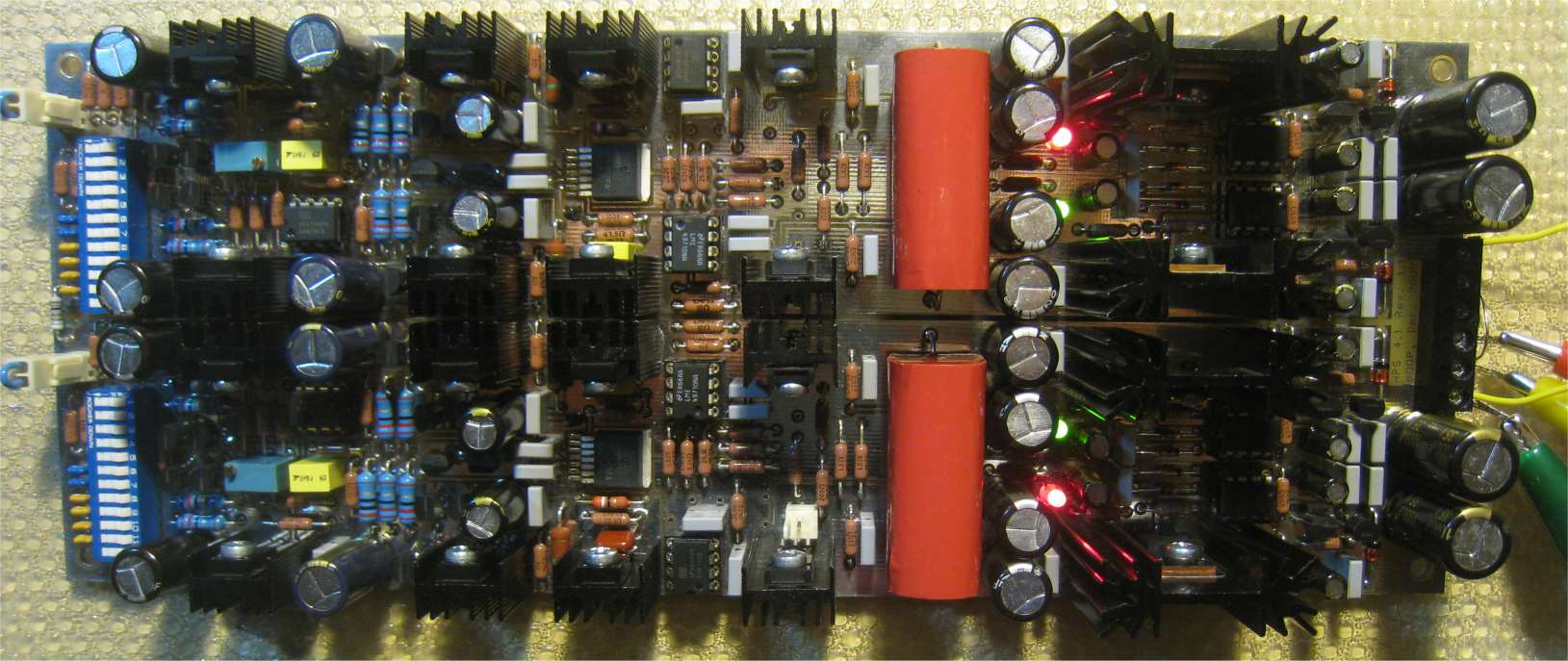
Here's a picture of the assembled HPS4.1 board.
And the new raw power supply board
HPS 4.1 before closing the lid
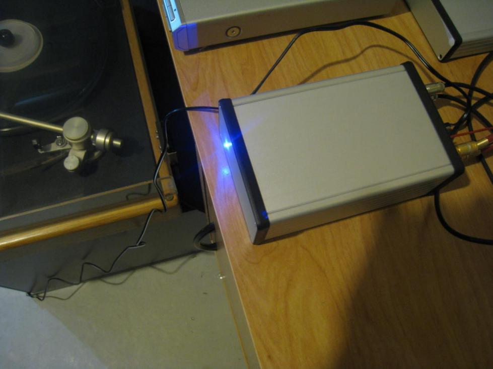
And added to the phone equipment stack (second from the bottom), ready for listening tests.
HPS 4.2
HPS 4.2 is both a refinement of the HPS 4.1 signal chain and a revamp of the HPS4.0 power supply. The original HPS4.0 used two pairs of inexpensive LM317/LM337 series regulators and current sources, to feed a pair of shunt local regulators. The core idea was that it makes little sense to build a relatively complex Jung regulator to feed opamp stages having anyway 60-80dB PSRR. A pair of inexpensive regulators will do a great job, in particular with good opamp supply pins decoupling. The low noise head amp stage is fed by the high performance shunt local regulators.
Unfortunately,there were a few errors in the original HPS 4.0 design, mostly related to the thermal budget. One problem with shunt regulators is that they need to provide the maximum current required by the load. In the particular case of the HPS 4.0 (and 4.1 as well), the head amp requires a maximum of +/-200mA (+/-8V output swing divided by 39 ohm the feedback resistor) plus the input and gain stages bias current, to a grand total of about 300mA. This current is required only under overload conditions otherwise, at nominal input, the current doesn't exceed +/-100mA. Also under normal/nominal conditions, the shunt regulator power device needs to carry the current balance; if the load takes 100mA, the power MOSFET takes 200mA and heats up, waiting for the rare occasions when the current balance is required by the load. 200mA by 17V makes 3.5W. Multiply this by four (there are four shunt regulators, in the dual mono construction) and add the power dissipation of the current sources (another 4W) and you get a disconcerting 18W dissipation, that heats up the board to the point where the (thermal) noise is affected.
The obvious solution is to pull the OPA552 stage out of the shunt regulators. The OPA552 opamp has enough PSRR to be fed straight from the LM317/LM337 power supply. Under these circumstances, the current drawn from the shunt regulators is almost constant, independent to the input signal/overload condition. The current sources and the shunt regulators can be designed for much lower current, that is, 150mA. The input stage takes about 100mA, so there's a 50mA margin flowing through the power MOSFETs, to a total dissipation of 6.4W. This is certainly manageable. The LM317/LM337 is able to deliver the 200mA current required by the OPA552, under overload conditions, but being series regulators the average impact on the power dissipation is minimal.
The shunt regulators used in the HPS 4.2 would certainly deserve a separate discussion, which I'll bring up in a separate page, time permitting. Although they are relatively simple, built around a high speed opamp and a power MOSFET, there are a few fine points about. First, the frequency compensation: I decided for the TMC (Transient Miller Compensation, Edmond Stuart's trademark) compensation method. TMC provides a relatively flat phase response of the control loop; this greatly enhances the transient response of the regulator. The unity loop gain is about 3MHz and the phase margin is over 80 degrees, for a 200mohm output electrolytic.
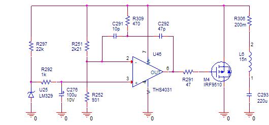
Shunt regulators require a pretty ugly trade between stability and noise. While the stability requires a HF compensation, the noise requirements are imposing very low values for the resistors in the feedback loop. Take a look at the schematic below:
R251 || R252 are pumping noise at the regulator output, as the C291, C292, R309 TMC compensation network drops the error amp gain only at HF. Therefore, there is a trade required, between the HF response of the regulator and the output noise. Unfortunately, simply shunting R251 with an electrolytic is not really an option; this makes the compensation network moot, and pushes the unity loop gain well past 10MHz. Finger crossed to keep the regulator stable...
The other method is to provide some PSRR in the load (here, the low noise input stage). The input stage already has a decent PSRR, but it can be improved by simply moving C206 and C207 (and the other equivalents, see the HPS 4.1 schematic) from the ground to the power supply.
Here's the head amp equivalent schematic. It can be used to simulate and analyze the effect of various parasitic elements.
As already mentioned, you would of course note that the CCS and folded cascode reference decoupling is now connected to the supply rails. While this change would, in the ideal case (zero PS output impedance, etc...) obviously increase the PSRR, it is not obvious what is going to happen in the real world, where components (mostly electrolytics) and PCB parasitics (R/L) exist.
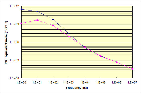
The metric for determining the effect was chosen as "Power Supply equivalent noise" shortly PSEN, that is, the amount of noise that the power supply has to inject, to match the headamp output noise; it is the output noise/PSRR as a function of frequency. Of course, the larger the better.
The results are attached (for the positive supply PS+; for PS- it's about the same). Rather surprisingly, the PSEN doesn't degrade at HF when using the supply decoupling. However, the improvement at lower frequency is obvious. The net result is that the noise corner frequency moved where it should be for a bipolar low noise stage, well under 10Hz (not that it was audible before, anyway :).
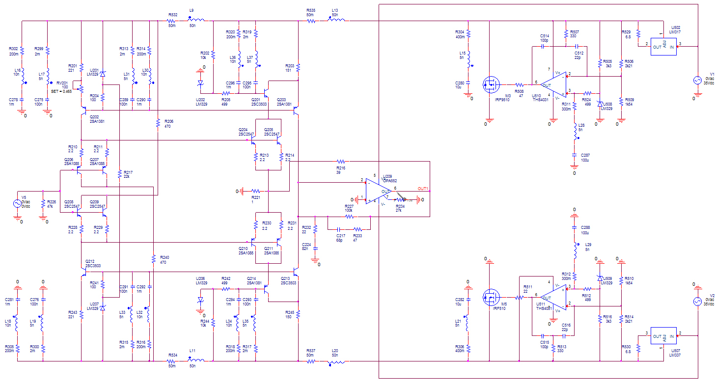
This being said, here are the HPS 4.2 signal chain and power supply board level schematics. You can download the Gerber files here. Due to a simpler power supply (four Jung regulators take quite some board space) and an optimized layout, the board is 8 sq. in. smaller than in HPS 4.1
The objective performances of HPS 4.2 are almost identical to HPS 4.1. See the Measurement section for the noise distribution. I simply replaced HPS 4.1 with the new HPS 4.2 board (see below) and it's now my favorite RIAA preamp (until the next design :)
One interesting conclusion was that the current sources feeding the shunt regulators have virtually no impact on the performances. A LM317/LM337 current source, a discrete current source, or even simple a resistor has virtually no measurable impact on the DC and AC performances. Funny enough though, a LM317/337 and a heatsink is cheaper than a power resistor :)
HPS 5.1
This page is growing longer and longer... If I only knew about the length and the popularity of these pages among DIY communities across the world, I would certainly structure the content in a much better way. A little late for that, I don't really want the make the already existing bookmarks invalid, while I don't have the mood and time to build redirections. Anyway, this chapter is probably the last one that I am writing regarding High Performance phono Stages (a.k.a. the HPS preamps). At this stage, it would probably be worth to review the entire journey.
The journey in the Silence Land started with an implementation of the original Colins preamp (HPS 1.0) then improving that design by adding a cascode in the low noise stage and a pair of Jung superregulators in a separate case (HPS 2.0).
Then continued by developing an innovative supersymmetrical headamp architecture, with no capacitors in the signal path, extending the dynamic range/overload margin to 32dBand a noise performance (using sorted JFETs) close to the 0.3nV/rtHz barrier (or a S/N ratio ref. 0.5mV of 88dB A-weighted), the HPS 3.1.
Then the HPS 4.x series followed, using low noise bipolar devices and an input bias cancelling method that allowed less than 50nA of DC current through the cartridge (so still no caps in the signal path). Various power supply options were employed, from the classic Jung regulators and local power buffers (HPS 4.1), to local high performance shunt regulators (TMC compensated to optimize the step response) as in HPS 4.2. The HPS 4.x series had a voltage equivalent noise of well under 0.3nV/rtHz, while the equivalent input current noise was measured under 5pA/rtHz, making them ideal for the most demanding MC cartridges (having low impedances). Also the distortions went significantly down compared to HPS 3.1.
DIYers across the world complained about several things: first, the lack of silk screens in the Gerber files available for downloading for free. Answer was always that I don't use silkscreens for the purpose of keeping the PCB prototyping costs low. While I do have the silkscreen and soldermask files, I don't publish them (as I don't publish BOMs) to discourage "blind copies". I am expecting from the prospective builders a certain level of skills and understanding of the schematics, allowing to correctly place the parts on the boards. That's never a huge trouble for an unicate build. Though, I know at least one case of a DIYer that took the time to create his own silkscreen design - congratulations!
Secondly, the complexity. True enough, the complexity grew significantly, from HPS 1.0 to HPS 4.2. So did the performance but, ultimately, how much complexity is really required without affecting the key performance metrics (noise, dynamic range, distortions, etc...)?
Third, the fixed gain of 60dB. Prospective builders are looking after a variable gain MC/MM phono stage, or at least a switchable gain, to accomodate MM or high output MC cartridges as well.
Meet the HPS 5.x series. I will include here only HPS 5.1, the latest and most advanced implementation.
HPS 5.1 uses the same concept of flat gain head amp since HPS 3.1. However, the head amp was greatly simplified. In a sense, the circle closed; the architecture is back to the simple Colins design, but with a few very important improvements.
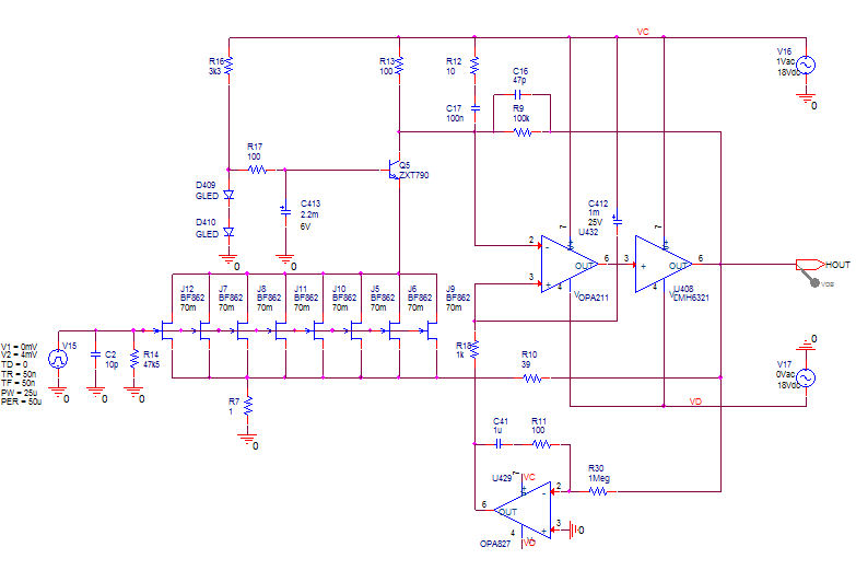
Eight BF862 low noise JFETs are paralleled in the input stage. BF862 is an excellent low noise JFET (0.8nV/rtHz, lower than 2SK170) currently in production at NXP and selling for pennies at all major semiconductors distributors (Mouser, etc...). BF862 has also larger Idss (and therefore transconductance) compared to 2SK170.
The JFETs are cascoded with a ZTX790 low noise power device. This device has a beta of 400 at 100mA and up, therefore it's current noise contribution to the overall noise balance is minimal. The cascode reference is provided by two LEDs, filtered by a 2200uF/100ohm cell. The JFETs Vds is kept to around 3V, so that they don't heat up (affecting the noise) and also no hot carriers injection occurs.
This input transconductance stage doesn't have the same large output impedance as in the HPS 3.x and HPS 4.x input stages, so there's no need to use a JFET input opamp; a bipolar SiGe OPA211 was selected, for the low noise, high open loop gain, high CMRR and high DC precision. Other options are possible here (LME49710, etc...), potentially the lead-lag frequency compensation R12/C17 has to be adjusted for stability. The OPA211 is unable though to deliver high current into the feedback network, so a LMH6321 power buffer was inserted. The LMH6321 can deliver up to 300mA continuous and 700mA shortcircuit, so it can not only feed the 39ohm feedback resistor up to 8V output (this is the worst case overload situation, but also a 9ohm feedback resistor, when the x10 head amp gain is selected.
An inverting servo, built around an OPA827 JFET input opamp is taking care of setting the opamp common mode voltage, so that the output offset is cancelled.
If you recall the HPS 1.0 on top of this page, the most important issue was the very poor PSRR. Any noise coming from the power supply gets amplified at the output. Even an extremely quiet power supply will still have something like 8 to 10 nV/rtHz noise; under these circumstances, even with a local RC filter, achieving 0.3nV/rtHz is impossible (at least because a large electrolitic still has hundreds of milliohm impedance, not low enough to short the power supply noise voltage, usually with a much lower output impedance. Therefore, the design should provide some decent PSRR. This is surprisingly easy to achieve by using a simple RC cell R12/C412. By referring both opamp inputs (in AC) to the positive power supply rail, the power supply noise is now appearing on the opamp common mode, being therefore rejected through the opamp CMRR. The overall head amp PSRR is down to better than -50dB.
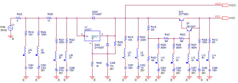
Now, we don't really want to build another complex Jung regulator to feed the head amp. Also using a local shunt regulator is not an option, as the regulator has to deliver up to 700mA, therefore running very hot. We would like to use a pair of inexpensive LM317/LM337 monolithic regulators. That's all the RIAA stages (built around opamps with high PSRR, and being not critical when it comes to noise, anyway) need. However, a LM317 regulator has a noise of several hundred nV/rtHz. Even with a 50dB PSRR this is still to high for an overall 0.3nV/rtHz design target. Therefore, the power supply noise has to be filtered out. A standard emitter follower power buffer (a.k.a. capacitance multiplier) does a pretty good job, however there's one thing that it can't filter out: the emitter follower Rbb. To avoid that contribution, we need some sort of local feedback loop, to obtain a significant lower equivalent Rbb. This is easily achieved by using a Sziklay configuration for the emitter follower. By including the power device in a current feedback loop, it's Rbb is effectively cancelled. It's now the low power device (which can be a low noise device) that dictates the equivalent Rbb of the emiteer follower. The power buffer schematic build around this concept (and with the parasitic elements included) is shown below. It is only the Q2 Rbb (a low noise device) that contributes to the power supply noise. Divided by the head amp PSRR, this contribution is negligible.
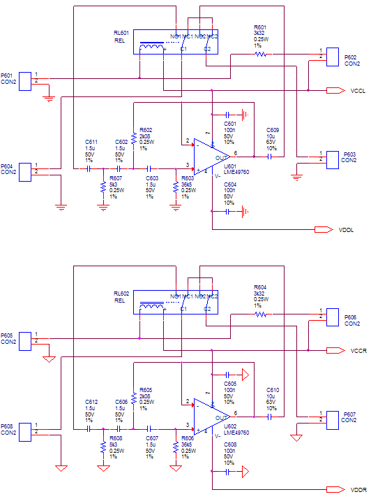
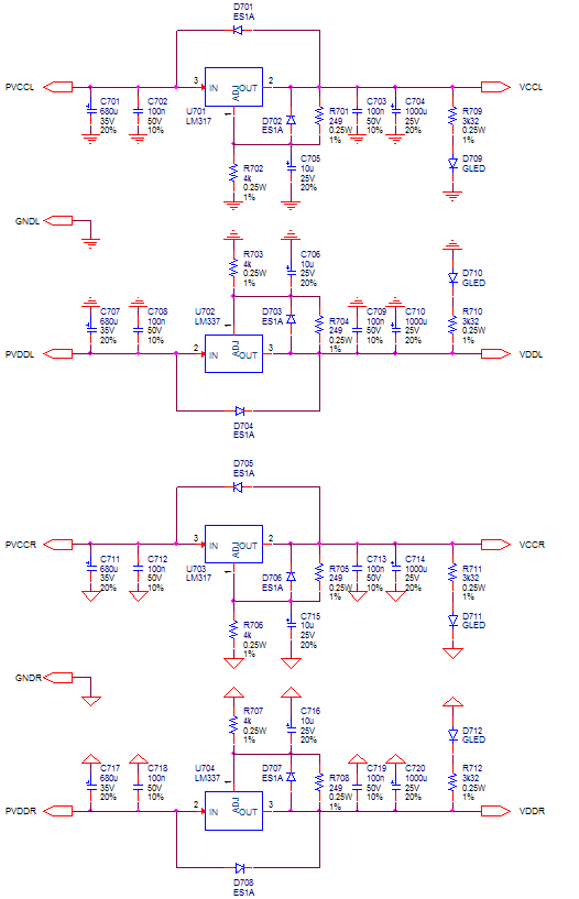
These being said, here's the HPS 5.1 signal path board level schematic (one channel only) and the HPS 5.1 power supply board level schematic. As you can easily spot, HPS 5.1 has switchable gain (x60dB and x48dB) via small signal NEC relays (the state of the art in low signal switching) implemented in a make-bfore-break schema. The JFET gate stoppers (1uH air core inductors) are mandatory; massively paralleled JFETs trend to oscillate on very high frequencies (over 100MHz).
I chosed to implement this project using SMD technology. It was my forst major SMD project and I have to say, it's easier and more fun than I was expecting. It is much easier to solder and eventually rework SMD parts (I am using 1206, that's what my eyes are allowing. The flip side is that SMD parts are usually (and absurdly) much more expensive than the equivalent leaded parts. In particular thin film resistors are usually available in 0.1% tolerance, for about $0.5-1 a pop. C0G precision caps are also very expensive, and polypropilene and styroflex film SMD parts virtually do not exist. The PCB has also to be professionally etched, it is unlikely for a dense SMD layout to be feasible for in house etching, by the common DIYer. The Gerbers for the HPS 5.1 construction are available here.
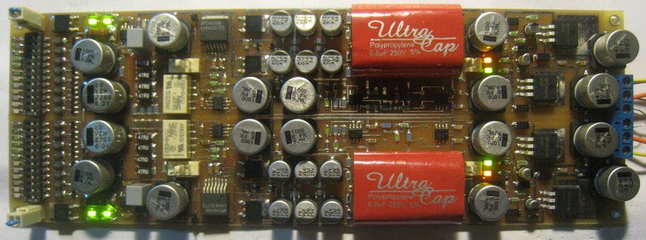
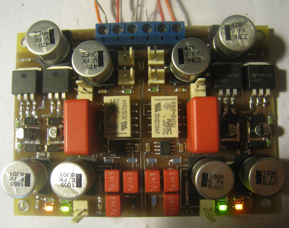
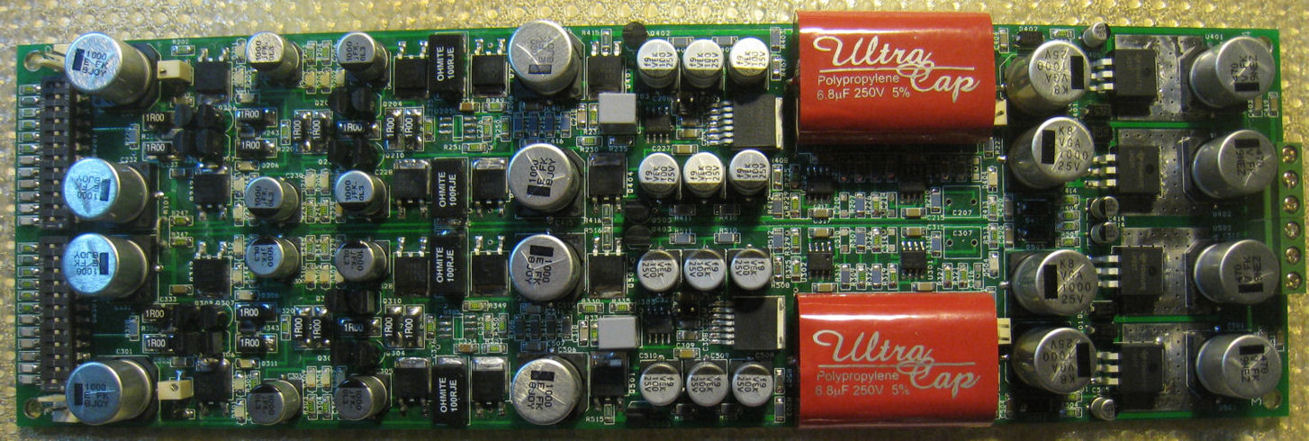
A picture of the full HPS 5.1 board:
The HPS 5.1 measurement results are available in the Measurements page.
I think I have already mentioned the rather strange effect of output slow fluctuations, unavoidable in low noise, high gain, DC coupled amps. These fluctuations are a direct result of the 10dB/decade increasing 1/f noise, coupled with the very high LF gain (80dB) of the RIAA designs, required for providing 60dB of gain at 1KHz. While these fluctuations can be safely neglected (one or more of the following stages up to the speakers will, sooner or later, act as a high pass filter removing any signals under a certain frequency, say 10Hz) it would be nice to remove these fluctuations at the RIAA preamp output. Of course, this somehow defeats the whole DC coupling concept ("no caps in the signal path") but then the high pass filtering is done when the signal is already in the hundreds of mV domain. It can be safely assumed that at these levels, any "damage" (don't ask what that is, I don't know) by the coupling film caps can be safely ignored.
But besides avoiding the very low frequency fluctuation, an output high pass filter may have another important functionality. How many of you were annoyed by the motor rumble, audible at high volumes, even for belt driven expensive turntables? And payed for a SAMA motor, only to fight to further acoustically isolate it from the turntable platter? And ever heard the annoying effect of an arm resonance, in the 10-20Hz domain?
There is a solution to avoid all of the above. A rumble filter is a high pass filter, with a cutoff frequency in the 10-15Hz domain. Such a filter poses some technical challanges, since while we certainly want to greatly attenuate any components under (say) 15 Hz, we need to minimize the impact at 20Hz, where the RIAA spec ends. This call for a high order high pass filter.
The most common solution is a Sallen Key 2nd order filter cell, built around a high voltage opamp, to conserve the dynamic range. Assuming a 18Hz 3dB corner frequency, such a cell will attenuate 12dB at 9Hz but unfortunately it affects the 20Hz response by almost 1dB, which is clearly audible. Lowering the corner frequency will unfortunately not provide enough attenuation at 10-12Hz where the most common arm resonances occur. Also, a second order filter can't provide a less than 20mS group delay (that is, according to Holman's work published by AES, the audibility threashold).
A higher order filter is required. Fortunately, the Sallen-Key cell has an extra degree of freedom, allowing adding anouther RC cell at the input, and providing a 3rd order high pass filter. Filter realisability criteria won't allow cascading this 3rd order cell in certain configurations, so the extra order comes to the price of flexibility, but for our purpose it works great. Assuming a 16 Hz corner frequency, it will attenuate by 18dB at 8Hz while keeping the 20Hz impact at under 0.2-0.3dB. And the group delay is under 20mS.
Here's the filter schematic. It is build as a separate unit, having it's own power supply (to provide the maximum flexibility) and allows swithcing the signal path via the NEC signal relays. Due to the separate power supply it can be easily integrated with an already existing RIAA preamp.
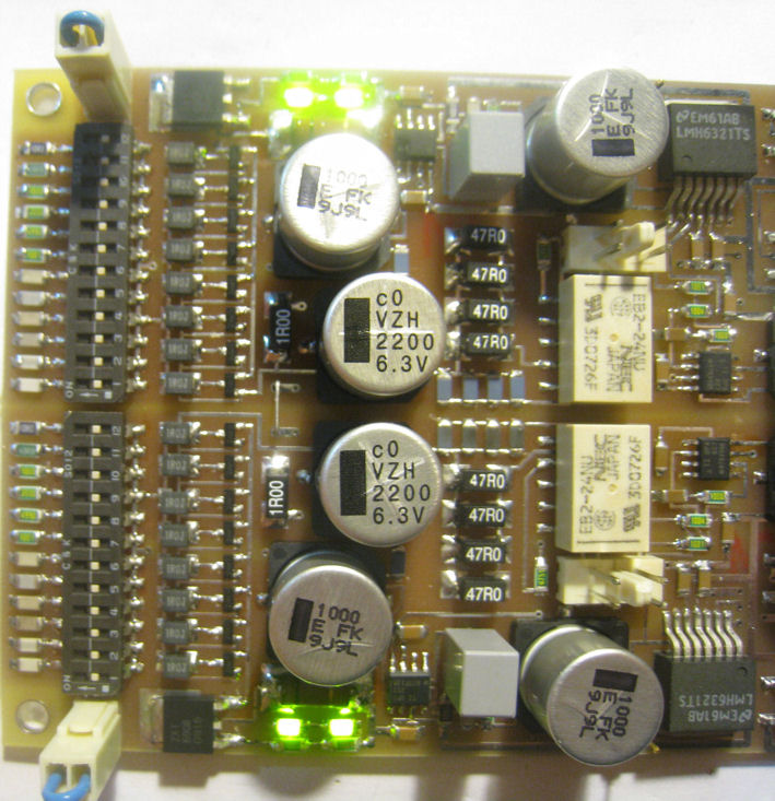
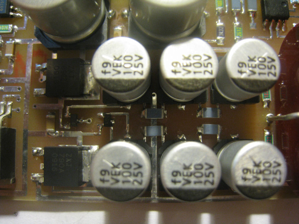
The HPS 5.1 head amp detail. Note the white small signal relays.
And the power buffer detail:
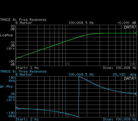
Here's a picture of the filter implementation and the measured (amplitude and phase) results. The HPF is built in SMD technology and requires 0.1% precision thin film resistors and carefully sorted caps in the filter sections. You can download the Gerber files here.
This pretty much concludes my journey into the land of silence. As a late development, I have decided to rebuild HPS 4.2 in SMD technology. By including the latest lesson learns from other designs (the low noise power buffer, split opamp + buffer instead of the OPA552) the results are no less exceptional, in particular in the harmonic noise department (that is, "hum") which twice lower compared to the HPS 4.2 leaded version of PCB). Here's a picture of the construction (now on a pro PCB with solder mask and legend). If enough interest will develop around this version, I'll be back and publish the full schematics and Gerbers.